Conductive semiconductor structures containing metal oxide regions

a metal oxide region and semiconductor technology, applied in semiconductor devices, semiconductor/solid-state device details, capacitors, etc., can solve the problems of unstable film for capacitor electrodes, unstable platinum layer, unstable metal/metal oxide structure, etc., to achieve enhanced surface area electrodes and stable metal/metal oxide structures

Inactive Publication Date: 2005-07-12
MICRON TECH INC
View PDF6 Cites 27 Cited by
  • Summary
  • Abstract
  • Description
  • Claims
  • Application Information

AI Technical Summary

Benefits of technology

[0011]The present invention provides a stable metal/metal oxide structure (e.g., a platinum/ruthenium oxide composite structure) for use in integrated circuits, e.g., capacitor electrodes. Such a metal/metal oxide composite struc

Problems solved by technology

Further, during high temperature processing of devices (e.g., high dielectric constant material formation processes) that include platinum conductive layers, stress occurs in the platinum layer.
Such stress may result in the formation of a discontinuous platinum layer, such as in the form of platinum islands, which are undesirable.
The formation o

Method used


Image

  • Conductive semiconductor structures containing metal oxide regions
  • Conductive semiconductor structures containing metal oxide regions
  • Conductive semiconductor structures containing metal oxide regions

Examples


Embodiment Construction

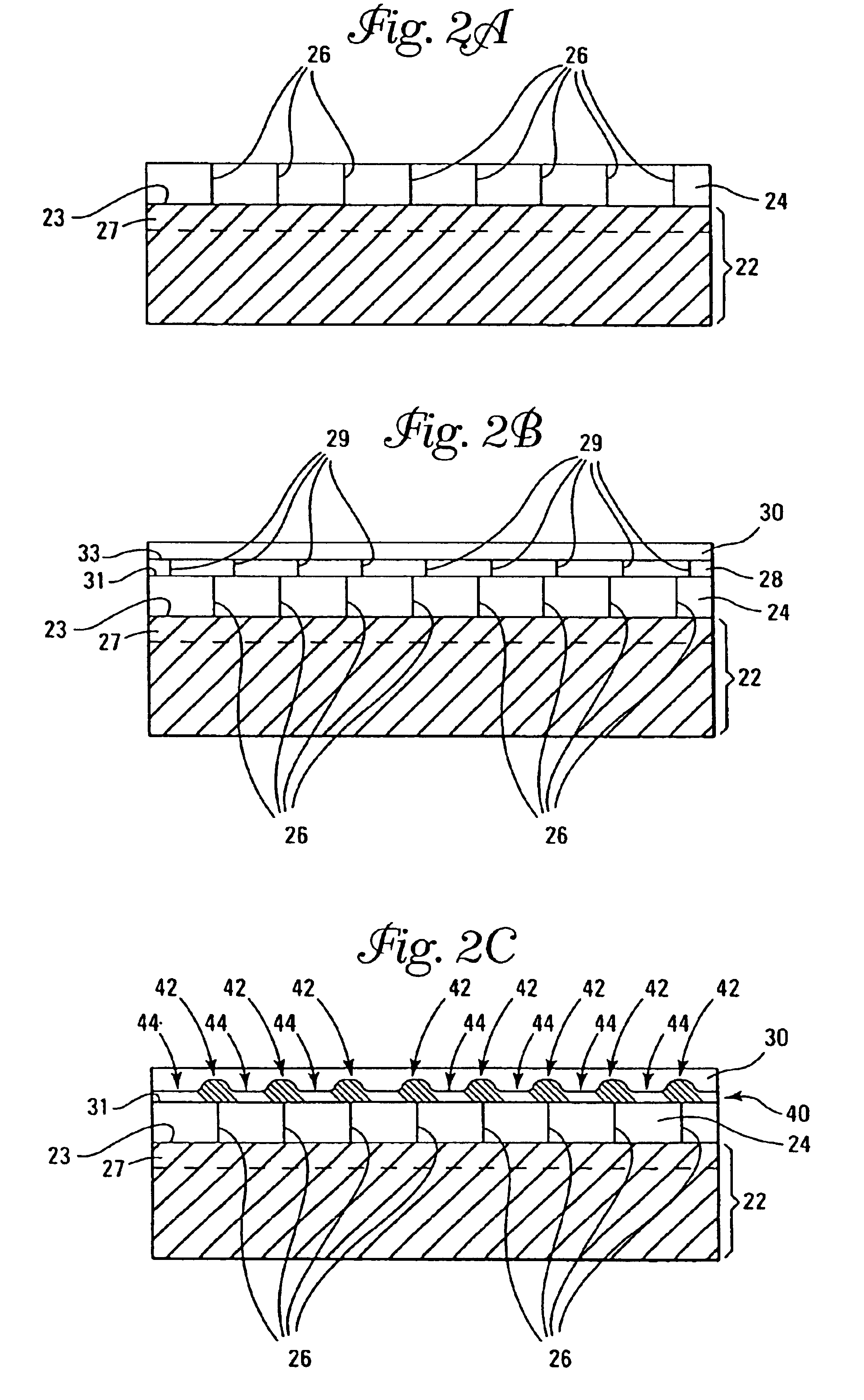
[0023]The present invention shall be generally described with reference to FIGS. 1-2. Thereafter, other embodiments, illustrations, and applications of the present invention shall be described with reference to FIGS. 3-4.

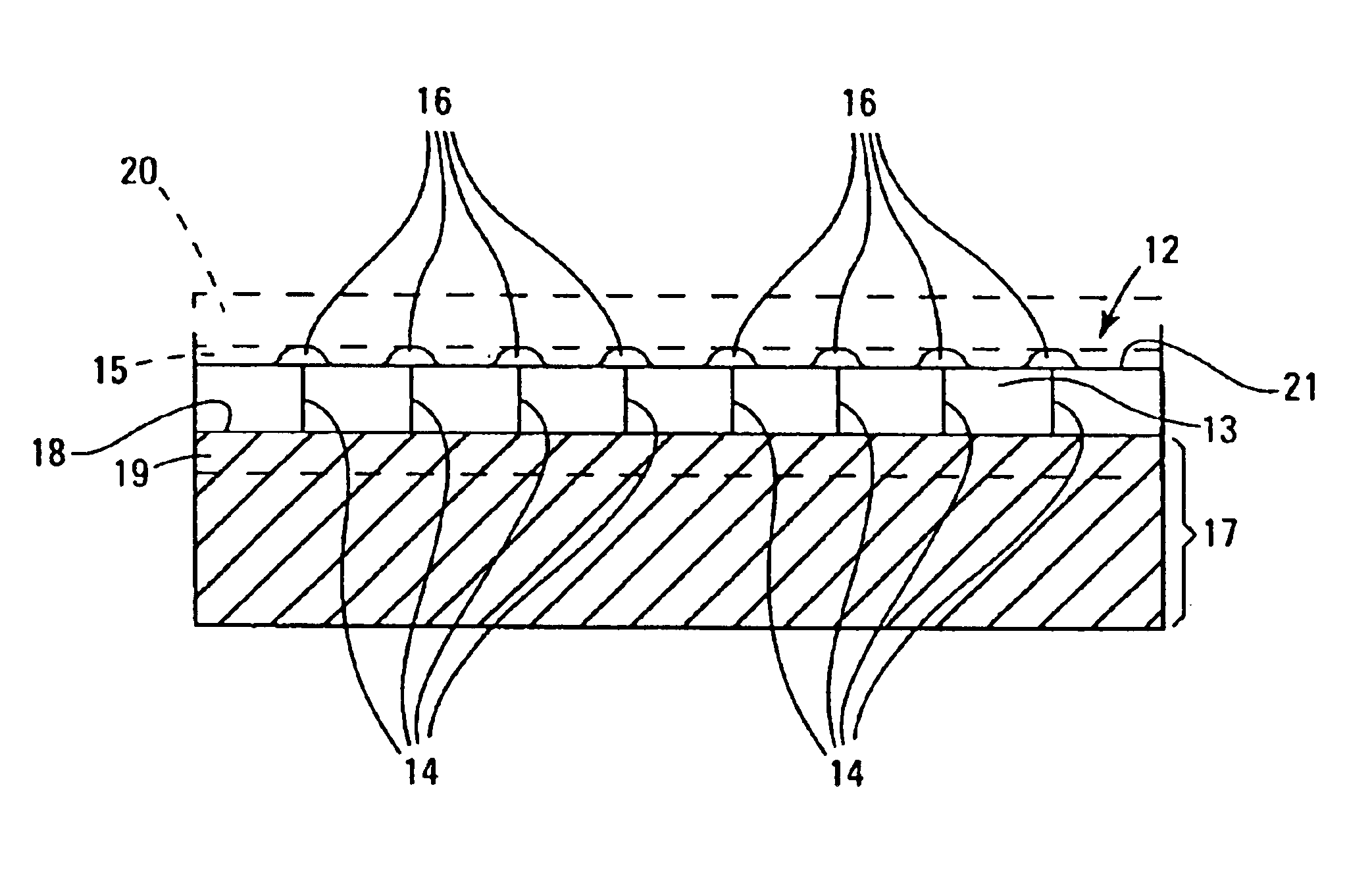
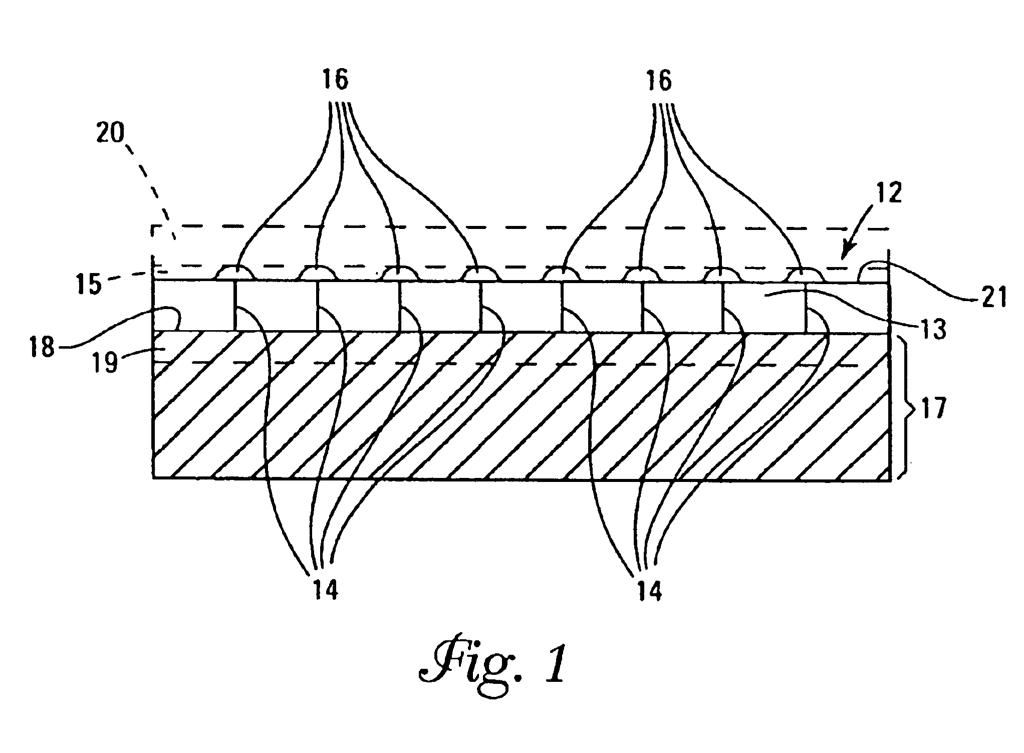
[0024]FIG. 1 illustrates a substrate assembly 17 and a metal / metal oxide composite structure 12 formed according to the present invention on a surface 18 of the substrate assembly 17, e.g., an oxygen-containing surface portion. FIG. 1 is illustrative of the use of a composite metal / metal oxide structure 12 for any application such as those requiring the benefits provided thereby as further described below. For example, the application may be a capacitor electrode application. As such an electrode, the composite metal / metal oxide structure 12 may be used to prevent oxygen diffusion through the electrode of the capacitor, provide an enhanced surface area, etc. Further, for example, the composite metal / metal oxide structure 12 may be used in the formation of storage ce...


PUM


Abstract

A method for forming a metal/metal oxide structure that includes forming metal oxide regions, e.g.. ruthenium oxide regions, at grain boundaries of a metal layer, e.g., platinum. Preferably, the metal oxide regions are formed by diffusion of oxygen through grain boundaries of the metal layer, e.g., platinum, to oxidize a metal layer thereon, e.g, ruthenium layer. The structure is particularly advantageous for use in capacitor structures and memory devices, such as dynamic random access memory (DRAM) devices.

Description

[0001]This is a division of application Ser. No. 09 / 711,206, filed Nov. 9, 2000, U.S. Pat. No. 6,534,357 , which is incorporated herein by reference.FIELD OF THE INVENTION[0002]The present invention relates to the preparation of semiconductor device structures. More particularly, the present invention pertains to methods of forming conductive structures such as electrode structures and the structures resulting therefrom.BACKGROUND OF THE INVENTION[0003]In the fabrication of integrated circuits, various conductive layers are used. For example, during the formation of semiconductor devices, such as dynamic random access memories (DRAMs), or any other types of memory devices, conductive materials are used in the formation of storage cell capacitors, and also may be used in interconnection structures, e.g., conductive layers in contact holes, vias, etc. For example, in the fabrication of integrated circuits including capacitor structures, conductive layers are used for capacitor electro...

Claims


Application Information

Patent Timeline
IPC IPC(8): H01L21/02H01L21/768H01L21/70
CPCH01L21/76888H01L28/75H01L28/55H01L28/84
Inventor BASCERI, CEMSANDHU, GURTEJ
Owner MICRON TECH INC
Why Eureka
Try Eureka