Interconnected networks of single-walled carbon nanotubes

a single-walled carbon nanotube and interconnected technology, applied in nanoinformatics, instruments, specific gravity measurement, etc., can solve the problems of lack of position and orientation control, major obstacles to commercial electronic applications, lack of precise atomic structure of swcnt control,

Inactive Publication Date: 2005-07-19
THE UNITED STATES OF AMERICA AS REPRESENTED BY THE SECRETARY OF THE NAVY
View PDF13 Cites 293 Cited by
  • Summary
  • Abstract
  • Description
  • Claims
  • Application Information

AI Technical Summary

Benefits of technology

[0007]The invention comprises an electronic device comprising an interconnected network of carbon nanotubes (CNTs) on the surface of a substrate, and two or more electrical leads. The network forms an electrical connection between the leads. The invention further comprises a device comprising an interconnected network of nanofilaments on the surface of a substrate, and two or more electrical leads.

Problems solved by technology

However, two major obstacles have stood in the way of commercial electronic applications.
The first obstacle is lack of position and orientation control.
The second problem is lack of control of the precise atomic structure of SWCNTs.
There has been little progress in solving either of these two problems that currently prohibit high yield device fabrication.
However, because of the limited current-carrying capacity of individual SWCNTs, many s-SWCNTs aligned side by side in a single device would be required in order to surpass the current drive of a Si device.
Such precise positioning of SWCNTs is beyond the capability of current growth and assembly technology and presents a major technological hurdle for carbon nanotube-based electronic applications.

Method used


Image

  • Interconnected networks of single-walled carbon nanotubes
  • Interconnected networks of single-walled carbon nanotubes
  • Interconnected networks of single-walled carbon nanotubes

Examples


example 1

[0039]Formation of interconnected networks—An iron-based catalyst for the nanotube growth was deposited on a Si wafer with a 250-nm-thick thermal oxide by dipping the substrates in a ferric nitrate nonahydrate isopropanol solution for 10 s followed by a 10 s rinse with hexane. The density of nanotubes was controlled by varying the concentration of the catalyst solution from 1.5 to 150 mg / L. Immediately after catalyst deposition, the samples were placed into a furnace and purged with a mixture of argon and hydrogen. The samples were then heated to 800° C. and annealed for 30 min. SWCNT growth was initiated by the introduction of ethylene (5 cm3 / min) into the Ar (600 cm3 / min)-H2 (400 cm3 / min) carrier gas flow for 10 min. The samples were then cooled in flowing Ar gas.

example 2

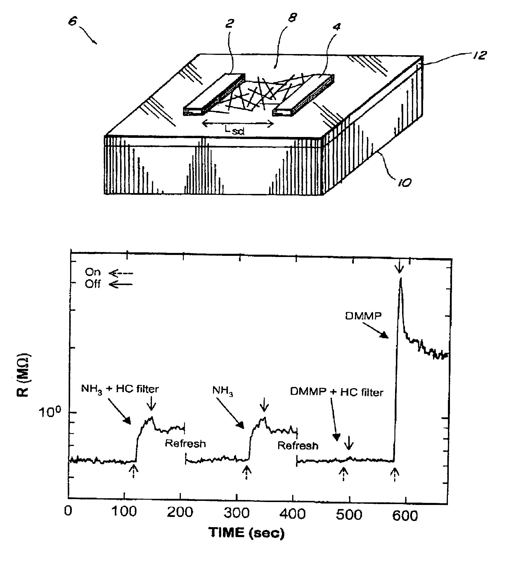
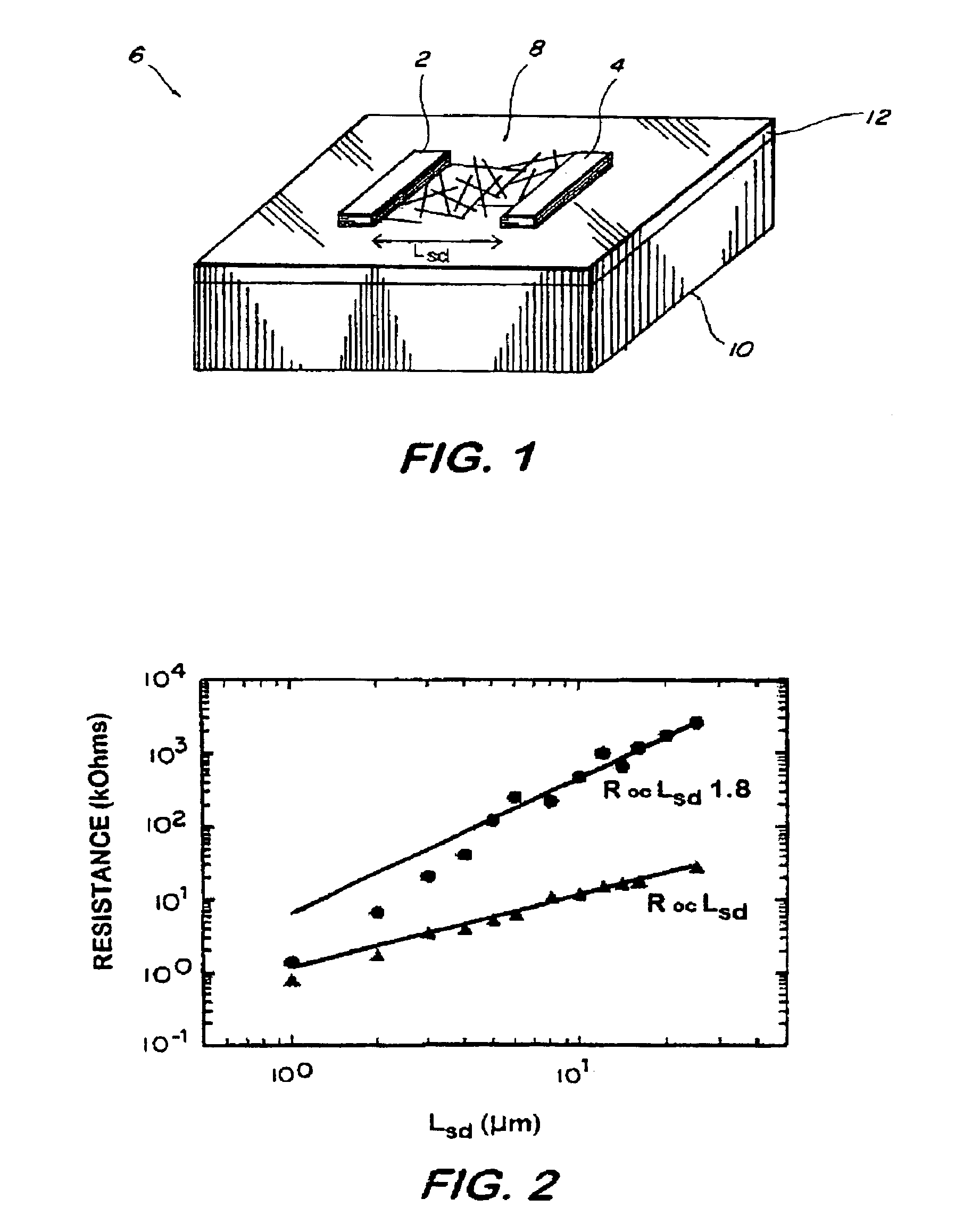
[0040]Fabrication of transistors—A schematic of the device is shown in FIG. 1. Source 2 and drain 4 electrodes were fabricated on the substrate 6 having the network 8 from Example 1 using optical lithography and lift-off of a 150-nm-thick Ti film. The regions of the devices between the source-drain electrodes were then covered with photoresist and the nanotubes outside this protected area were removed by using a CO2 snow jet. Finally, the protective photoresist was removed. The Si wafer 10, having a SiO2 layer 12, was used as the gate. The device geometry was varied with the source-drain channel length, Lsd, ranging from 1 to 25 μm and the channel width, W, ranging from 35 to 100 μm. An atomic force microscope (AFM) image of a CNT network in the region between the source-drain electrodes was made. Such images and AFM line profiles were used to determine the diameter (d), density (ρ), and length (L) of the nanotubes where ρis defined as the number of CNTs per unit area. For these gro...

example 3

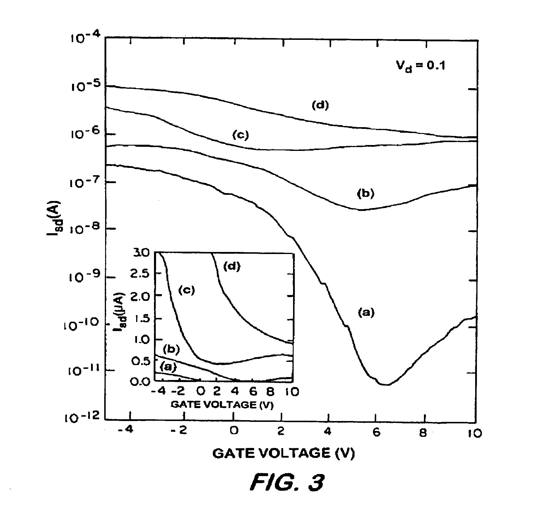
[0041]Electrical properties of transistors—The transistors from Example 2 were tested in a vacuum probe station. Networks were electrically conducting for CNT densities exceeding ˜0.3 μm−2. For most of the devices, the average nanotube length, , was much shorter than Lsd, which means that the source-drain current flowed through a series of inter-nanotube contacts.

[0042]The geometric scaling of the device resistance is shown inFIG. 2 which plots the log of the source to drain resistance versus log(Lsd) for two sets of devices corresponding to ρ=10 and 1 μm−2. The resistance data for the 10 μm−2 network scaled linearly with channel length with a sheet resistance of 108 kΩ / square. The resistance data for the 1 μm−2 network scaled nonlinearly with channel length, and a least squares power law fit to the data for Lsd≧5 μm yielded R∝L1.8. This nonlinear scaling is an indication that the network is approaching the percolation threshold where nonlinear effects are expected. Note that the sh...


PUM

PropertyMeasurementUnit
thickaaaaaaaaaa
thicknessesaaaaaaaaaa
concentrationaaaaaaaaaa

Abstract

An electronic device having an interconnected network of carbon nanotubes on the surface of a substrate, and two or more electrical leads. The network forms an electrical connection between the leads.

Description

[0001]is application claims the benefit of U.S. Provisional Patent Application No. 60 / 456,536 filed on Mar. 24, 2003 and U.S. Provisional Patent Application No. 60 / 465,218 filed on Apr. 25, 2003, both incorporated by reference.BACKGROUND OF THE INVENTION[0002]1. Field of the Invention[0003]The invention relates generally to materials useful as components of electronic devices such as transistors.[0004]2. Description of the Prior Art[0005]Because of their unique structural, mechanical and electrical properties, materials containing single-wall carbon nanotubes (SWCNTs) have been developed for electronic and sensor applications. However, two major obstacles have stood in the way of commercial electronic applications. The first obstacle is lack of position and orientation control. Such control is necessary for high-yield device fabrication. The second problem is lack of control of the precise atomic structure of SWCNTs. SWCNTs are currently produced with a range of diameters and differ...

Claims


Application Information

Patent Timeline
Patent Type & Authority Patents(United States)
IPC IPC(8): H01L51/05H01L51/30G01N27/12G01N27/414H01L21/00
CPCB82Y10/00G01N27/127G01N27/4146H01L51/0048H01L51/0545Y10S977/75Y10S977/842H10K85/221H10K10/466
Inventor SNOW, ERIC S.NOVAK, JAMIE P.CAMPBELL, PAUL M.
Owner THE UNITED STATES OF AMERICA AS REPRESENTED BY THE SECRETARY OF THE NAVY
Why Eureka
Try Eureka