

Semiconductor device and its manufacturing method
- Summary
- Abstract
- Description
- Claims
- Application Information
AI Technical Summary
Benefits of technology
Problems solved by technology
Method used
Image

Examples
first embodiment
[0077](First Embodiment)
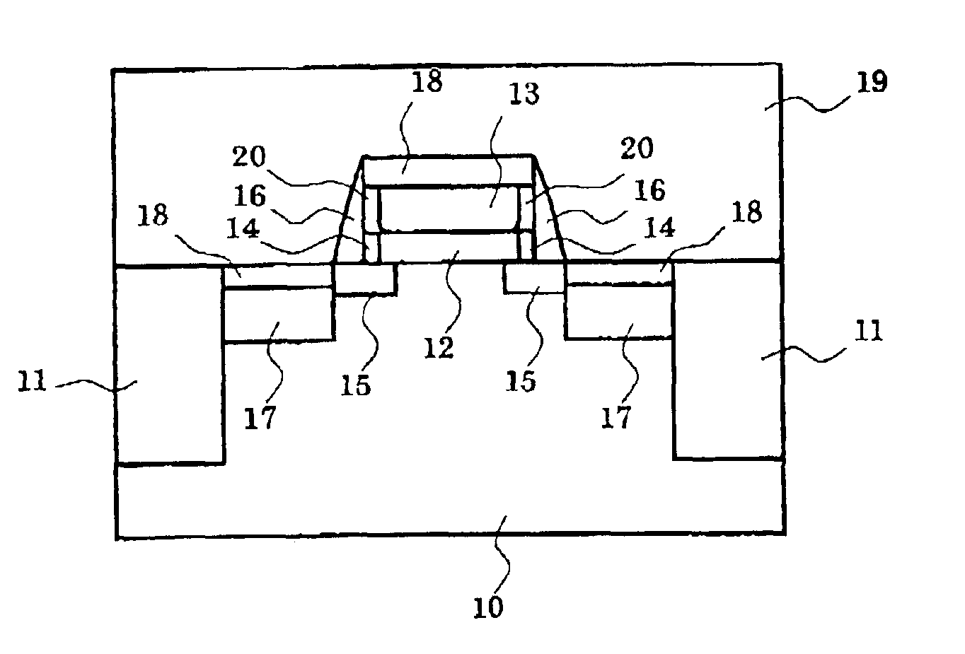
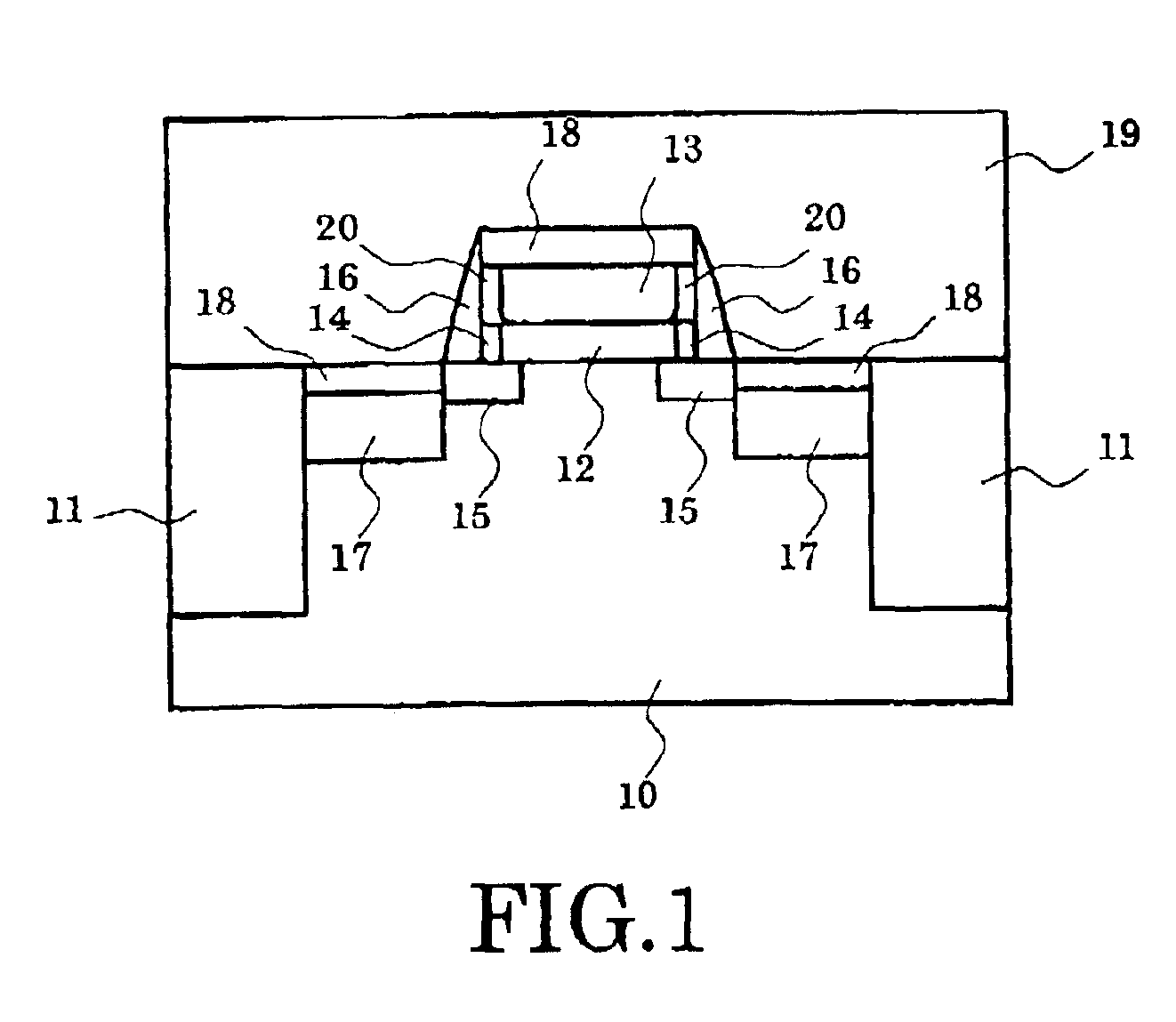
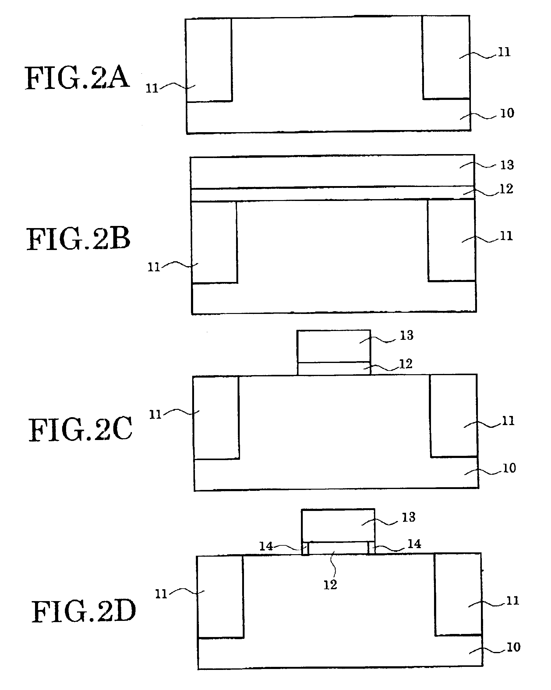
[0078]FIG. 1 is a schematic diagram which exemplifies the principal part cross-sectional structure of the semiconductor device according to the first embodiment of the invention.
[0079]That is, the semiconductor device shown in this figure is an example obtained by applying the invention to MISFET structure. Isolation regions 11 are formed near the surface of the semiconductor layer 10, and the transistor is formed in the semiconductor portion separated by these regions 11. This transistor has the gate structure where the laminating of the gate insulating film 12 and the gate electrode 13 is carried out on the semiconductor layer 10.
[0080]Side walls 16 are formed in the both sides of the gate structure, and the source region 17 and the drain region 17 are formed in the outside. And the source extension region 15 and the drain extension region 15 are extending out from these source drain regions 17 towards the bottom of the gate electrode 13, respectively.
[0081...
second embodiment
[0133](Second Embodiment)
[0134]Next, the second embodiment of the invention will be explained.
[0135]FIG. 6 is a schematic diagram which exemplifies the principal part cross-sectional structure of the semiconductor device concerning the embodiment. The same symbols are given to the similar elements as what was mentioned above about FIGS. 1 through 5 about this figure, and detailed explanation is omitted.
[0136]Also in MISFET of this example, the gate insulating film 22 is formed of high dielectric material with a dielectric constant higher than a silicon oxide, like the case of the first embodiment. As mentioned above with reference to FIG. 1, as such high dielectric materials, lanthanoid elements, the oxides of various kinds of metals in addition to this, or these silicates can be used.
[0137]Also in this embodiment, the high concentration region 14 is provided in the both ends of the gate insulating film 22, like the first embodiment, and thus the content of nitrogen becomes higher i...
third embodiment
[0157](Third Embodiment)
[0158]Next, the third embodiment of the invention will be explained.
[0159]FIG. 9 is a schematic diagram which exemplifies the principal part cross-sectional structure of the semiconductor device concerning this embodiment. The same symbols are given to the similar elements as what was mentioned above about FIGS. 1 through 8D also about this figure, and detailed explanation is omitted.
[0160]MISFET of this example has substantially the similar structure as the example mentioned above about the first embodiment. However, the formation method of the high concentration region 34 is different. That is, also in this embodiment, the gate insulating film 12 is formed of high dielectric material with a dielectric constant higher than a silicon oxide, like the case of the first embodiment As mentioned above with reference to FIG. 1 as such a high dielectric material, lanthanoid elements, the oxides of various kinds of metals, or these silicates can be used.
[0161]Also in...
PUM
 Abstract
Description
Claims
Application Information