Method for probing a semiconductor wafer

a technology for semiconductor wafers and probes, applied in individual semiconductor device testing, semiconductor/solid-state device testing/measurement, instruments, etc., can solve problems such as latching, junction defects, and generation of photo emission, so as to avoid reverse or unnatural images of the wafers, avoid difficulties, and reduce the time required

Inactive Publication Date: 2005-08-09
BELL SEMICON LLC
View PDF2 Cites 117 Cited by
  • Summary
  • Abstract
  • Description
  • Claims
  • Application Information

AI Technical Summary

Benefits of technology

[0011]One aspect of the present invention relates to facilitating the application of power and signal probes to an IC on a semiconductor wafer for testing and failure analysis. Other aspects of the invention relates to avoiding the difficulties and reducing the time required to place the tips of power and signal probes on selected conduction points of an IC of a semiconductor wafer, avoiding reverse or unnatural images of the wafer while placing the power probes on the semiconductor wafer for backside failure analysis, and avoiding the disadvantages of precisely placing the tips of relatively long power and signal probes adjusted by microscopic mechanisms located at the opposite end of the arm from the tip.

Problems solved by technology

The type of faults which typically generate a photo emission include junction defects, contact spiking, hot electrons, latch-up, poly filaments, and substrate damage and contamination.
The effectiveness of optical failure analysis techniques used on the front side of the wafer is diminished because of the increased complexity of many ICs.
The increasing number of layers makes photo emission microscopy from the front side of the wafer difficult, if not impossible, because of the lack of visibility of the photo emissions from the front side of the wafer.
Instead, the photon emissions pass between or are scattered around the metal interconnection layers, preventing the detection of photo emissions from the surface of the wafer or otherwise decreasing the accuracy of locating the fault.
The effectiveness of the optical failure analysis techniques used on the front side of the wafer is diminished because the additional metal interconnect layers obstruct the visibility of faults in the active devices.
Application of the failure analysis techniques on the back side of the wafer is complicated with existing wafer probing techniques.
This process is complicated in terms of eye-to-hand coordination since the video image is a reverse image of the wafer from the viewpoint of a normal viewing.
The process of connecting the probes to the semiconductor device is generally time consuming and prone to error.
Application of the failure analysis techniques on the front side of the wafer is also complicated with existing wafer probing techniques.
Because of the relatively long arm of the probes and their cantilevered extension from the adjustment mechanism, the movement of the tip of the probes is magnified, which makes placement of the probe tip very difficult, tedious and time-consuming to precisely and accurately position the probe tip on the desired connection point of the IC.
Consequently, connecting the probes to the semiconductor device for front side failure analysis techniques is generally time consuming and prone to error.

Method used


Image

  • Method for probing a semiconductor wafer
  • Method for probing a semiconductor wafer
  • Method for probing a semiconductor wafer

Examples


Embodiment Construction

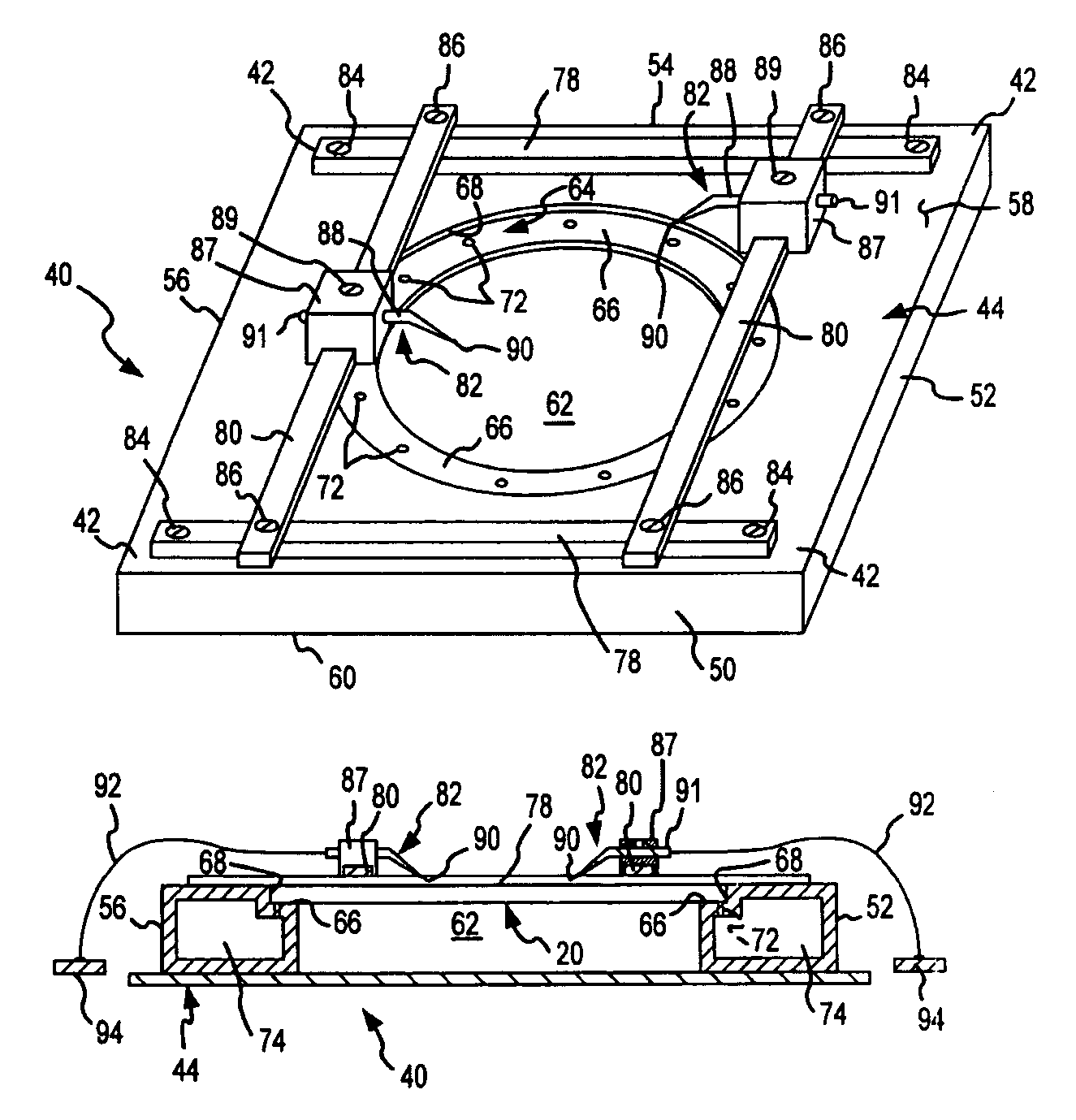
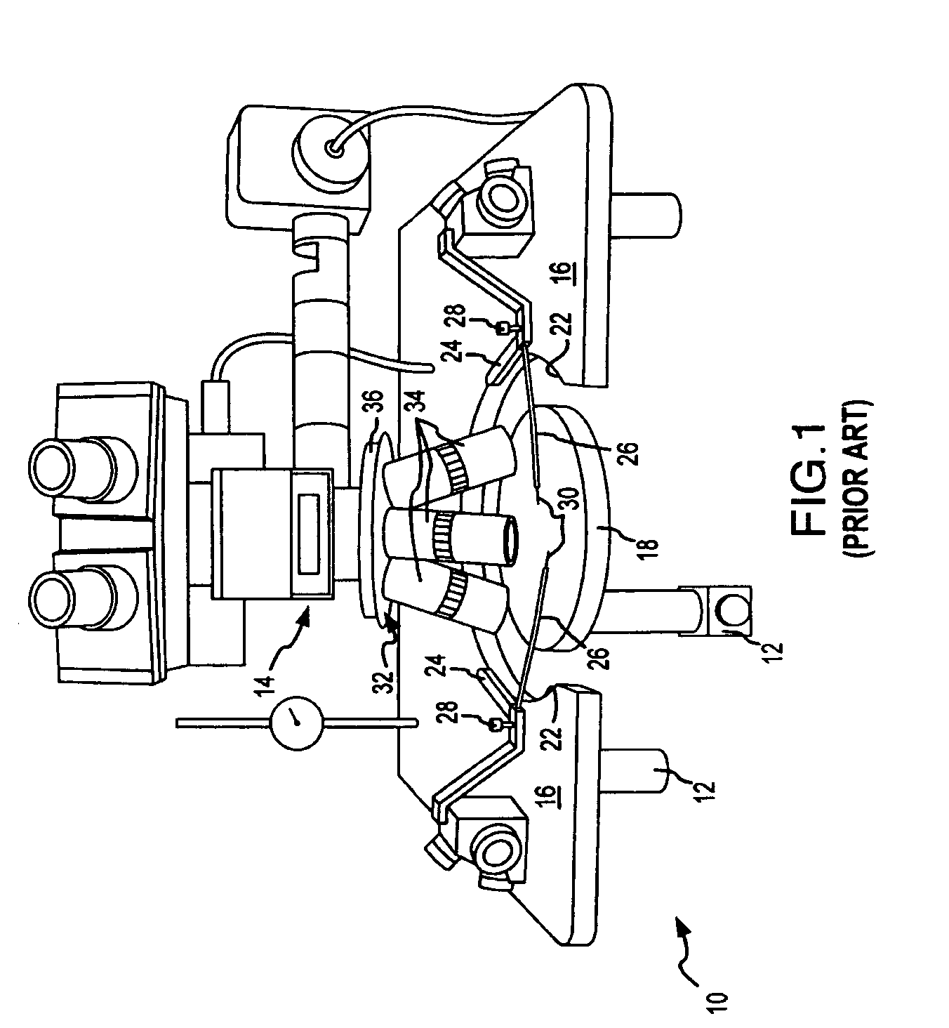
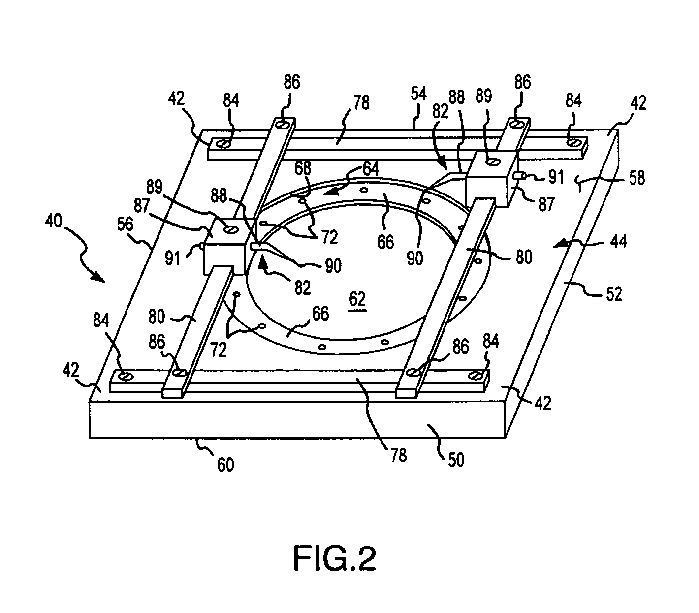
[0021]A typical test station 10 is shown in FIG. 1 to include frame structure 12 which supports and positions a microscope 14, a platen 16 and a chuck 18 to hold a wafer 20 (FIGS. 4 and 5) which is undergoing testing or analysis. The platen 16 has a circular opening 22 for the chuck 18 to move toward and away from a turret 24 of the microscope 141 though the platen 16. The wafers 20 and other devices such as printed circuit boards, typically referred to as the device under test (DUT) are connected to the chuck 18 or to the platen 16. The circular opening 22 is sized to permit wafers 20 and other printed circuit boards (not shown) to be attached to the platen 16 and to be positioned relative to the microscope 14 for convenient observation. Both the platen 16 and the chuck 18 typically move independently. The chuck 18 and the microscope 14 typically move in the X, Y, and Z directions. The platen 16 typically moves only in the Z direction.

[0022]Probes 24 are typically connected to the ...


PUM

PropertyMeasurementUnit
poweraaaaaaaaaa
photoemission detection microscopeaaaaaaaaaa
pressureaaaaaaaaaa

Abstract

A semiconductor wafer is placed into a probe fixture with a front side of the wafer facing up. Power and signal probes are then placed on an integrated circuit (IC) formed on the front side of the wafer. The probe fixture is retained at a test station either in a upright or an inverted position for testing and optical failure analysis. The probe fixture includes a position adjustment mechanism to locate the entire probe above the wafer and to more precisely position a tip of the probe on the IC. Optical failure analysis techniques are performed on the front side or the back side of the wafer while the wafer is retained in the test fixture and the probes are connected to the IC.

Description

FIELD OF THE INVENTION[0001]This invention relates to probing semiconductor devices formed on wafers, as typically accomplished when applying power and / or signals to the semiconductor devices when testing them or when conducting failure analysis. More particularly, the present invention relates to a new and improved probing fixture for placing contact probes on a semiconductor wafer which makes it easier to position the probes, which makes spurious movement of the probes less likely, and which facilitates applying power and signals to the wafer when performing failure analysis using optical techniques from the back side of the wafer.BACKGROUND OF THE INVENTION[0002]Failure analysis of a semiconductor device is done with a variety of techniques used to locate, analyze, and identify faults in the device. The semiconductor integrated circuit (IC) or chip is typically formed on a silicon substrate using a layering technique which results in a multilayered device composed of various laye...

Claims


Application Information

Patent Timeline
Patent Type & Authority Patents(United States)
IPC IPC(8): H01L21/66G01R31/28G01R31/311
CPCG01R31/311G01R31/2831G01R31/2893
Inventor FYFIELD, MARGARET S.
Owner BELL SEMICON LLC
Why Eureka
Try Eureka