Wavelength converter, method of manufacturing wavelength converter and optical device using the same
a technology of wavelength converter and manufacturing method, which is applied in the direction of optical waveguide light guide, light demodulation, instruments, etc., can solve the problems of large insertion loss, decrease of conversion efficiency of polymeric wavelength converter, and large difference between the thickness of channel-shaped waveguide and the diameter of the core of single-mode optical fiber
- Summary
- Abstract
- Description
- Claims
- Application Information
AI Technical Summary
Benefits of technology
Problems solved by technology
Method used
Image
Examples
embodiment 1
[0040](Embodiment 1)
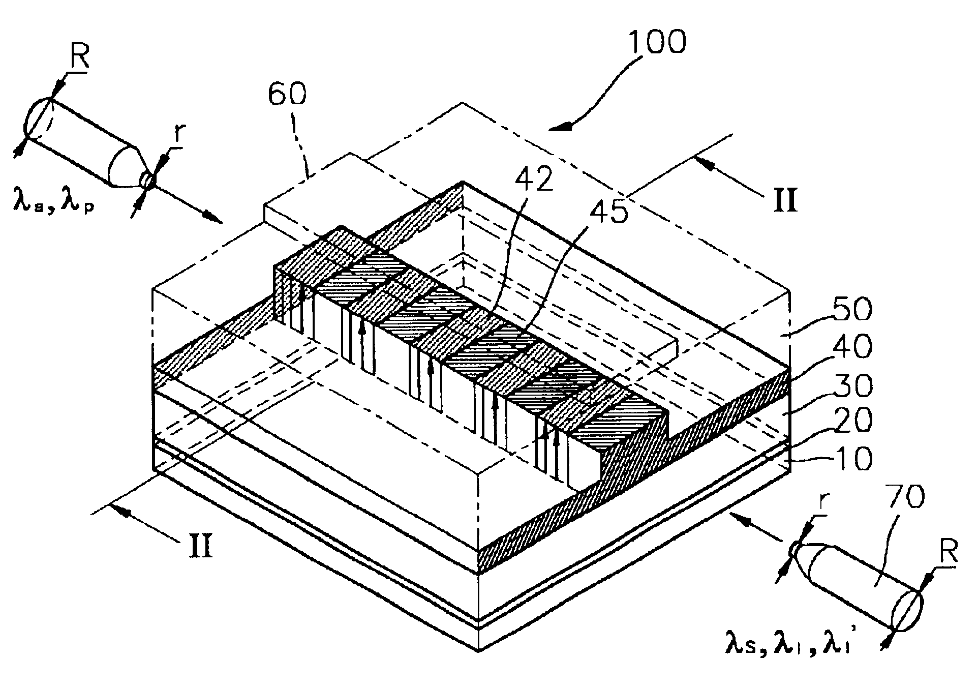
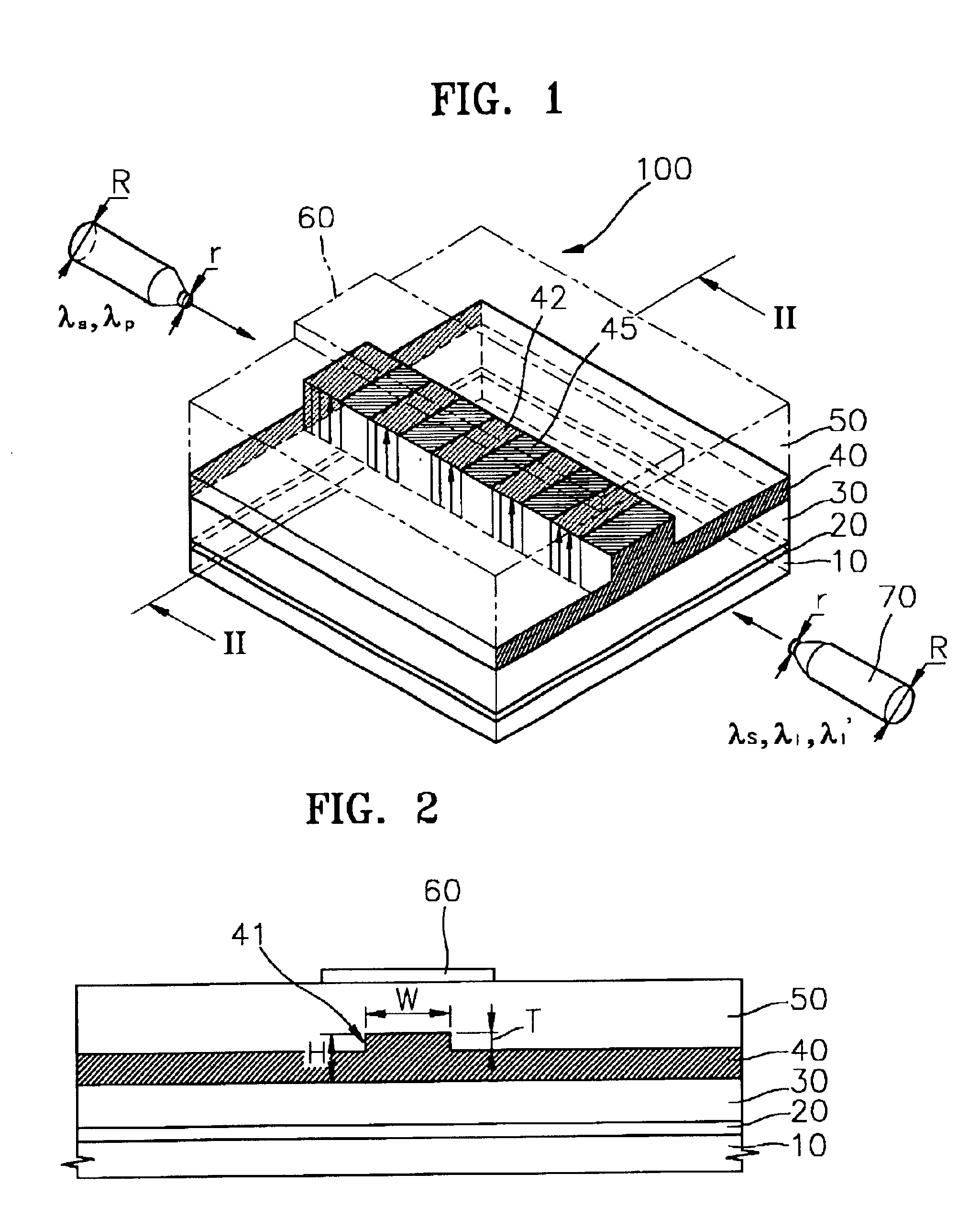
[0041]FIG. 1 is a perspective view of a wavelength converter according to an embodiment of the present invention, and FIG. 2 is a cross-sectional view taken along line II—II of FIG. 1.
[0042]As shown in FIGS. 1 and 2, a first electrode 20 and a polymeric lower cladding layer 30 are formed sequentially on a semiconductor substrate 10. Here, a silicon wafer having the diameter of about 3 inches may be used for the semiconductor substrate 10, and the first electrode 20 may be formed by evaporating metals in which a chrome (Cr) layer having the thickness of about 50 Å and gold (Au) having the thickness of about 1000 Å are stacked, under a high vacuum of 1.0×10⁻⁶ torr. The chrome (Cr) layer composing the first electrode 20 is formed so as to improve a force in which the Au layer adheres to the semiconductor substrate 10.
[0043]After that, a linear polymeric layer, i.e., NA061 (manufactured by Norland Intl.) layer is coated with 7.0 Krpm spinning for 30 seconds on the fi...
embodiment 2
[0069](Embodiment 2)
[0070]FIG. 6 is a block diagram of an optical device having a wavelength converter according to the present invention. Referring to FIG. 6, the optical device according to the present invention includes an inputting portion 150, a wavelength converter 100, and an outputting portion 200.
[0071]The inputting portion 150 is comprised of a light source 110, an optical amplifier 120, a variable filter 130, and a photocoupler 140. Pump light is used for the light source 110. In the case of a DFG mode, a variable wavelength laser diode having the wavelength of 780 nm is used for the light source 110, and in the case of a cascade mode, a variable wavelength laser diode having the wavelength of 1.55 μm is used for the light source 110. The optical amplifier 120 amplifies the inputted pump light at a predetermined level. The variable filter 130 variably transmits wavelength and removes spontaneous emission noise from the pump light amplified by the optical amplifier 120. Th...
embodiment 3
[0076](Embodiment 3)
[0077]FIG. 7 is a block diagram of a dispersion compensation optical device using the wavelength converter according to the present invention. Referring to FIG. 7, the dispersion compensation optical device includes an inputting portion 250, a wavelength converter 100, a dispersion compensator 280, and a wavelength feedback portion 290.
[0078]The inputting portion 250 includes an optical amplifier 252, a variable filter 254, and an optical equalizer 256. The optical amplifier 252 amplifies signal light dispersed through optical fiber 251 at a predetermined level. The variable filter 254 removes the spontaneous emission noise from the amplified signal light, and the optical equalizer 256 equalized the intensity of signal light having different wavelengths.
[0079]As described above, the wavelength converter 100 converts the wavelength of the inputted signal light so as to minimize insertion losses. Here, spectrum of signal light λi converted by the wavelength convert...
PUM
 Abstract
Description
Claims
Application Information


