Selectively applying resolution enhancement techniques to improve performance and manufacturing cost of integrated circuits

a technology of enhancement and resolution, applied in the field of fabricating semiconductor chips, can solve the problems of increasing the static power consumption of the chip, the low process technology of tens of millions of transistors fabricated with 130 nm and below, and the large off-state leakage current of fast transistors, so as to reduce the gate length of critical transistors and reduce the delay through critical transistors

Inactive Publication Date: 2005-08-09
SYNOPSYS INC
View PDF20 Cites 238 Cited by
  • Summary
  • Abstract
  • Description
  • Claims
  • Application Information

AI Technical Summary

Benefits of technology

[0017]In a variation on this embodiment, performing the first set of aggressive RET operations involves decreasing gate lengths of the critical transistors to reduce delay through the critical transistors. Moreover, performing the second set of less aggressive RET operations involves adjusting gate lengths of the other non-critical transistors to limit static power consumption of the other non-critical transistors caused by off-state leakage current.

Problems solved by technology

Unfortunately, as feature size continues to decrease, off-state leakage current from transistors increases, which can greatly increase the static power consumption of a chip.
Hence, circuits with tens of millions of transistors fabricated with 130 nm and below process technology have to tradeoff performance with off-state leakage current.
However, these fast transistors also have large off-state leakage currents.
Hence, the increased performance resulting from this additional drive current, Ion, is accompanied by a corresponding increase in off-state current, Ioff, which increases the static power consumption of the chip.
This increased static power consumption can be especially troublesome for portable computing devices with limited battery life.
Also note that the use of resolution enhancement techniques (RETs) to reduce gate lengths can increase mask cost and increase mask writer time because RETs increase the complexity of the layout.
Moreover, RETs can also increase the time required to perform mask inspection.

Method used


Image

  • Selectively applying resolution enhancement techniques to improve performance and manufacturing cost of integrated circuits
  • Selectively applying resolution enhancement techniques to improve performance and manufacturing cost of integrated circuits
  • Selectively applying resolution enhancement techniques to improve performance and manufacturing cost of integrated circuits

Examples


Embodiment Construction

Wafer Fabrication Process

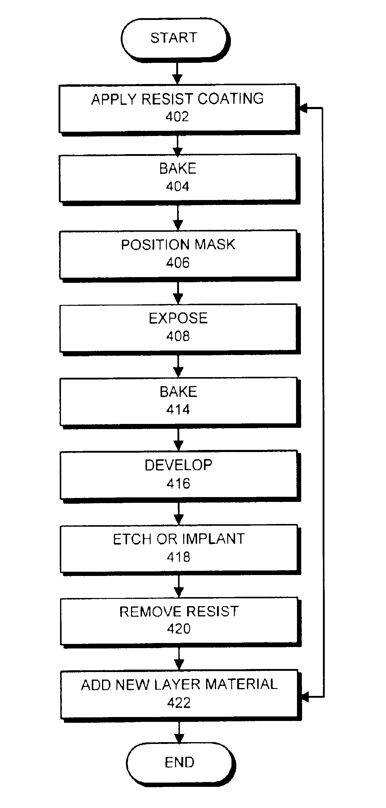
[0030]FIG. 4 is a flow chart illustrating the operation of the system that performs a wafer fabrication process in accordance with an embodiment of the invention. The system starts by applying a photoresist layer to the top surface of a wafer (step 402). Next, the system bakes the photoresist layer (step 404). The system then positions a mask over the photoresist layer (step 406), and exposes the photoresist layer through the mask (step 408). Next, the system optionally bakes the wafer again (step 414) before developing the photoresist layer (step 416). Next, either a chemical etching or ion implantation step takes place (step 418) before the photoresist layer is removed (step 420). (Note that in the case of a lift-off process, a deposition operation can take place.) Finally, a new layer of material can be added and the process can be repeated for the new layer (step 422).

[0031]Note that in a double exposure process that makes use of a phase shift mask, the ...


PUM


Abstract

One embodiment of the present invention provides a system that applies resolution enhancement techniques (RETs) selectively to a layout of an integrated circuit. Upon receiving the layout of the integrated circuit, the system identifies a plurality of critical regions within the layout based on an analysis of one or more of, timing, dynamic power, and off-state leakage current. The system then performs a first set of aggressive RET operations on the plurality of critical regions. The system also performs a second set of less aggressive RET operations on other non-critical regions of the layout.

Description

BACKGROUND[0001]1. Field of the Invention[0002]The invention relates to the process of fabricating semiconductor chips. More specifically, the invention relates to a method and an apparatus to reduce the amount of resolution enhancement applied to a die by selectively modifying transistor gate lengths to improve the speed of critical transistors that affect timing of a circuit, while limiting the static power consumption of other transistors in the circuit[0003]2. Related Art[0004]Recent advances in integrated circuit technology have largely been accomplished by decreasing the feature size of circuit elements on a semiconductor chip. Reducing the feature size increases the speed at which circuits can operate and increases the number of circuit elements that can be incorporated onto a semiconductor chip.[0005]Unfortunately, as feature size continues to decrease, off-state leakage current from transistors increases, which can greatly increase the static power consumption of a chip. He...

Claims


Application Information

Patent Timeline
Patent Type & Authority Patents(United States)
IPC IPC(8): G01R31/26G06F9/45G06F17/50H01L21/66
CPCG06F17/5081G06F30/398
Inventor PRAMANIK, DIPANKARSANIE, MICHAEL
Owner SYNOPSYS INC
Why Eureka
Try Eureka