Episeal pressure sensor and method for making an episeal pressure sensor

a pressure sensor and episeal technology, applied in the field of episeal technology, can solve the problems of large die area, large die area, and large die area, and achieve the effects of accurate pressure sensor, reduced cost of pressure sensor production, and good control

Inactive Publication Date: 2005-08-16
ROBERT BOSCH GMBH
View PDF9 Cites 96 Cited by
  • Summary
  • Abstract
  • Description
  • Claims
  • Application Information

AI Technical Summary

Benefits of technology

[0009]The method of the present invention offers high quality single crystal silicon membranes for piezoresistor implants, and provides methods for building capacitive sensors. The finished membranes are pure silicon, without oxide plugs, and the technique avoids some problems that may occur with oxide-sealed membranes.
[0012]The technique involves making a membrane that is sealed. The sensor may be built on a small die because a pyramidal-shaped pit opposite the deformable membrane is not necessary. Therefore the cost of producing pressure sensors may be reduced. Additionally, a method according to an exemplary embodiment of the present invention may be very good at controlling the thickness and the size of the membrane of the pressure sensor, and may thereby produce a more accurate pressure sensor.

Problems solved by technology

This method may be described as both reliable and mature, but the backside processing can be expensive and can consume large amounts of die area.
One problem with this technique is that cutting a hole from the back of the wafer can consume a lot of space on the die.
The larger die size increases the cost of the pressure sensor.
Therefore, a 10% error in the thickness may cause about a 30% error in the strength of the membrane, which may lead to about a 30% error in the sensitivity of the pressure sensing device using the membrane.
In other words, a small error in the thickness may lead to a large error in the pressure measurement.
Therefore, the size (i.e. the diameter) and the thickness of the membrane can be hard to control and may therefore impair the accuracy of the pressure sensor constructed in accordance with conventional methods.
This technique may be limited, however, by crystal defects in the epitaxial silicon grown over the porous silicon.

Method used


Image

  • Episeal pressure sensor and method for making an episeal pressure sensor
  • Episeal pressure sensor and method for making an episeal pressure sensor
  • Episeal pressure sensor and method for making an episeal pressure sensor

Examples


Embodiment Construction

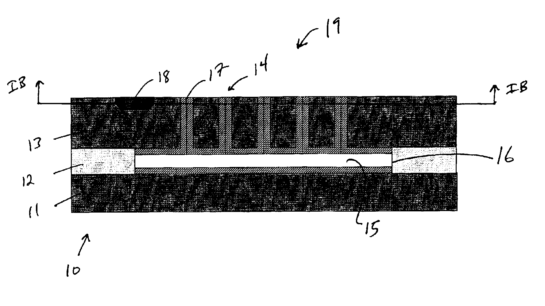
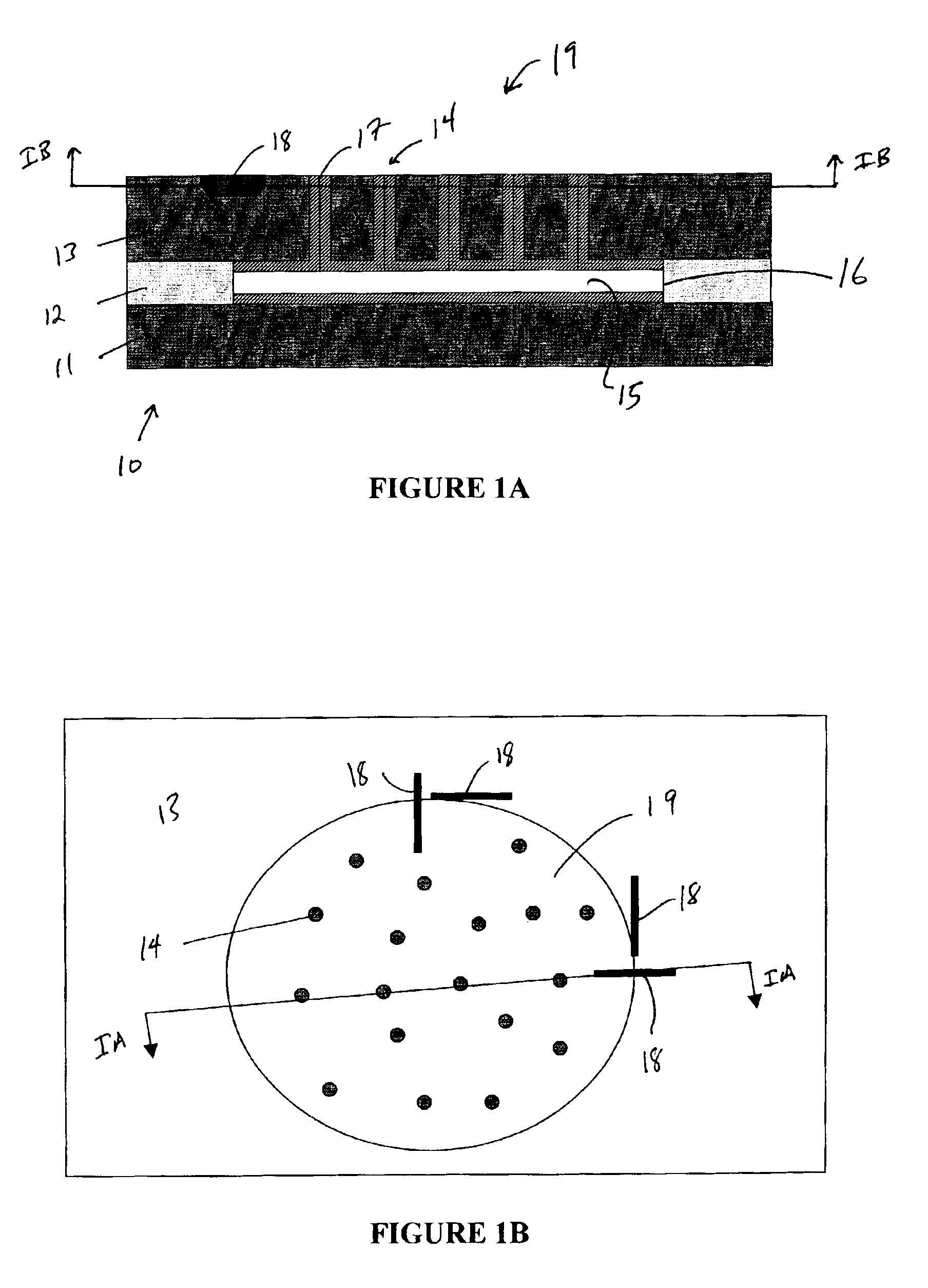
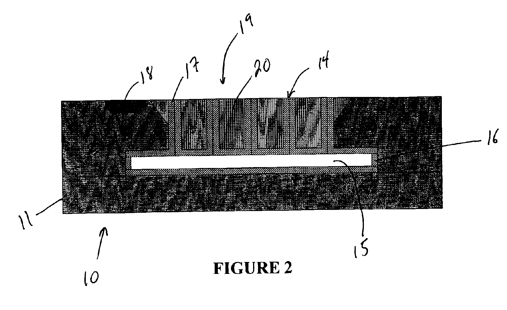
[0023]In an exemplary embodiment of the present invention, pressure sensor device structures are built with episeal technology. Episeal as used herein means sealing using an epitaxial reactor. An epitaxial reactor is used to deposit silicon epitaxially. Epitaxially deposited silicon follows the form of the silicon on which it is deposited, and may be either monocrystalline silicon or polycrystalline silicon. Epipoly is used herein to refer to epitaxially deposited polycycrystalline. Applications include both low cost and high accuracy pressure sensors. Sensing with both piezoresistive and capacitive techniques may be supported by the present invention. The pressure sensor according to an exemplary embodiment of the present invention may be built in at least two ways, either by growing epitaxial silicon or by using a bonded wafer, for instance an SOI (Silicon on Insulator) wafer. The proposed method may control the thickness by the epitaxial deposition parameters, or by bonding and g...


PUM

PropertyMeasurementUnit
distanceaaaaaaaaaa
thickaaaaaaaaaa
thickaaaaaaaaaa

Abstract

A method for making a pressure sensor by providing a wafer including a base silicon layer, a buried sacrificial layer, and a top silicon layer. The top silicon layer is arranged over the buried sacrificial layer and the buried sacrificial layer is arranged over the base silicon layer. Etching vents through the top silicon layer to the buried sacrificial layer and removing a portion of the buried sacrificial layer. Depositing silicon to seal the vents and arranging a strain gauge or a capacitance contact on the wafer. A method for making a pressure sensor including providing a bulk wafer and depositing a sacrificial layer on the bulk wafer. Depositing silicon on the sacrificial layer and the bulk wafer to form an encapsulation layer. Etching vents through the encapsulation layer to the sacrificial layer and removing the sacrificial layer. Closing the vents with a silicon deposition and arranging a strain gauge or a capacitance contact on the encapsulation layer. A pressure sensing device including a substrate, an encapsulation layer with vents, and voids between the substrate and the encapsulation layer. A portion of the encapsulation layer above the voids forms a membrane and deposited silicon plugs fill the vents. A strain gauge or a top capacitive contact arranged on the membrane.

Description

FIELD OF THE INVENTION[0001]The present invention generally regards episeal technology. More particularly, the present invention regards episeal pressure sensors in which an episeal membrane spans a cavity in a wafer.BACKGROUND INFORMATION[0002]Pressure sensors may be used in cars, for example, to measure oil pressure, to measure tire pressure, and to measure brake fluid pressure. Additionally, there are numerous non-automotive applications for pressure sensors.[0003]Pressure sensors have been made using wafers by conventional micromachining methods. For example, pressure sensors have been built by thinning sensing membranes from the back of wafers. This method may be described as both reliable and mature, but the backside processing can be expensive and can consume large amounts of die area. The membrane may be formed by etching a wafer from the back until it is a predetermined distance from a front surface of the wafer and then stopping the etch. The distance from the front face m...

Claims


Application Information

Patent Timeline
Patent Type & Authority Patents(United States)
IPC IPC(8): B81B3/00G01L9/00H01L29/84
CPCB81C1/00047G01L9/0045G01L9/0054G01L9/0073B81B2201/0264B81B2203/0127B81C2201/0109B81C2201/0177B81C2203/0145
Inventor PARTRIDGE, AARONLUTZ, MARKUS
Owner ROBERT BOSCH GMBH
Why Eureka
Try Eureka