Hafnium nitride buffer layers for growth of GaN on silicon

a technology of hafnium nitride and buffer layer, which is applied in the direction of crystal growth process, polycrystalline material growth, transportation and packaging, etc., can solve the problems of limiting the efficiency of such devices, layer contains structural defects, stacking faults, and point defects, etc., to achieve superior diffusion resistance, closer lattice match, and the effect of superior diffusion resistan

Inactive Publication Date: 2005-08-16
RGT UNIV OF CALIFORNIA
View PDF23 Cites 21 Cited by
  • Summary
  • Abstract
  • Description
  • Claims
  • Application Information

AI Technical Summary

Benefits of technology

[0008]The invention described herein demonstrates that hafnium nitride is an effective buffer layer for GaN on Si, with epilayer quality comparable to typical results achieved using AlN buf

Problems solved by technology

However, the poor material quality of GaN severely limits the efficiency of such devices.
The layer contains structural defects such as, threading dislocations, stacking faults, and point defects.
These defects degrade the film's morphology and optical and electrical properties.
However, Si substrates present additional challenges for GaN growth.
Thick (>1 μm) GaN epilayers often crack upon cooling to room temperature due to the severe tensile stress induced by the ˜35% sm

Method used


Image

  • Hafnium nitride buffer layers for growth of GaN on silicon
  • Hafnium nitride buffer layers for growth of GaN on silicon
  • Hafnium nitride buffer layers for growth of GaN on silicon

Examples


Embodiment Construction

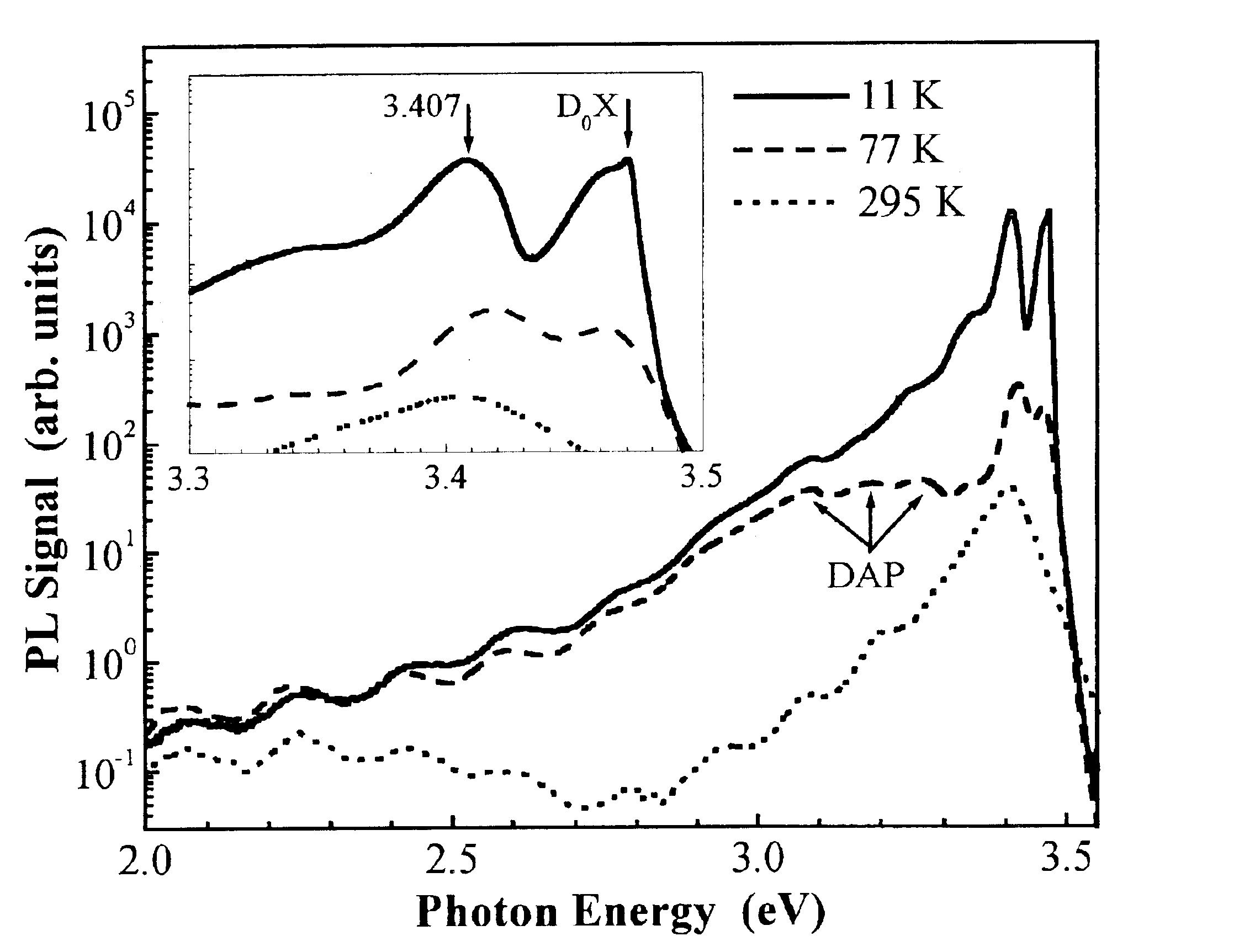
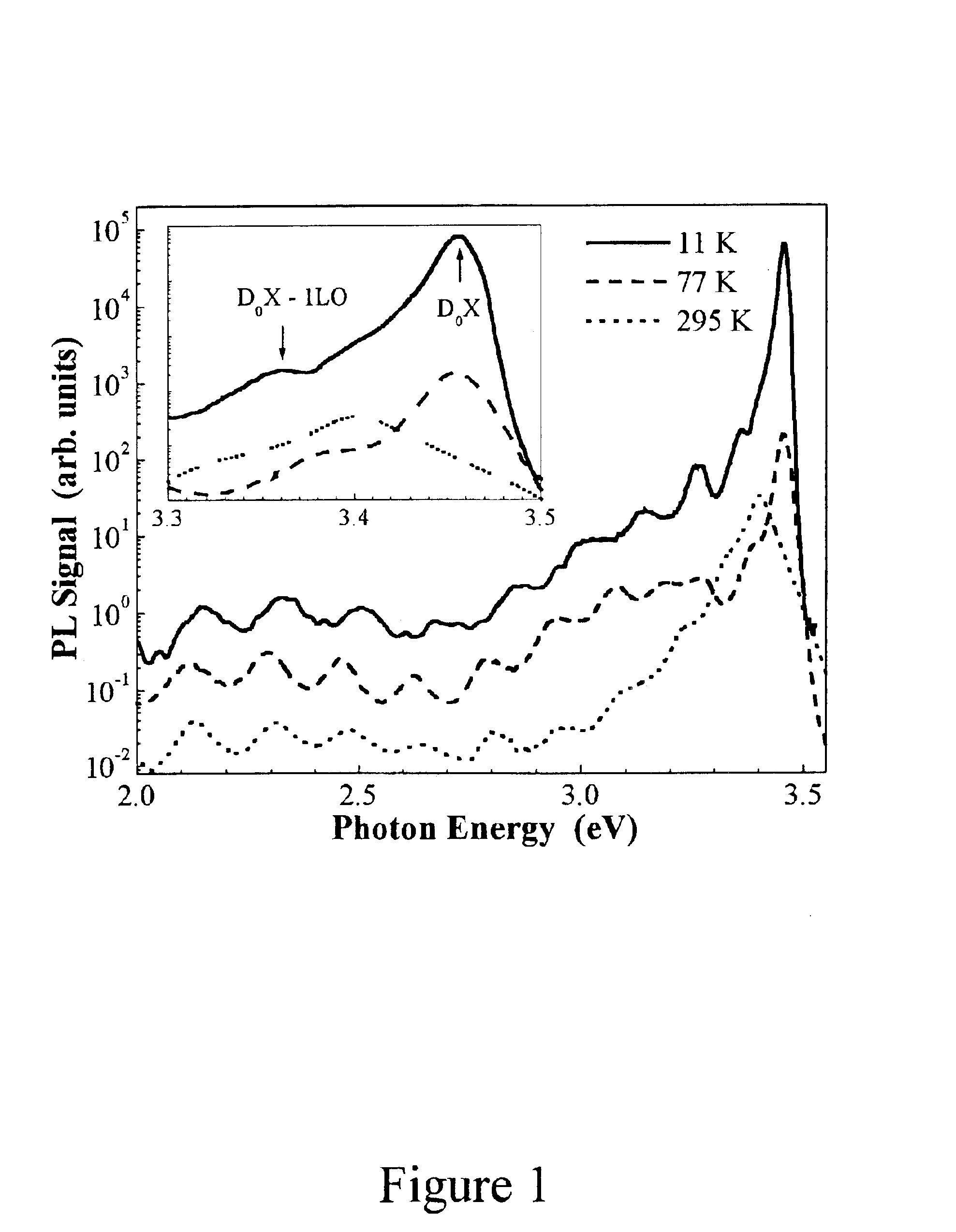
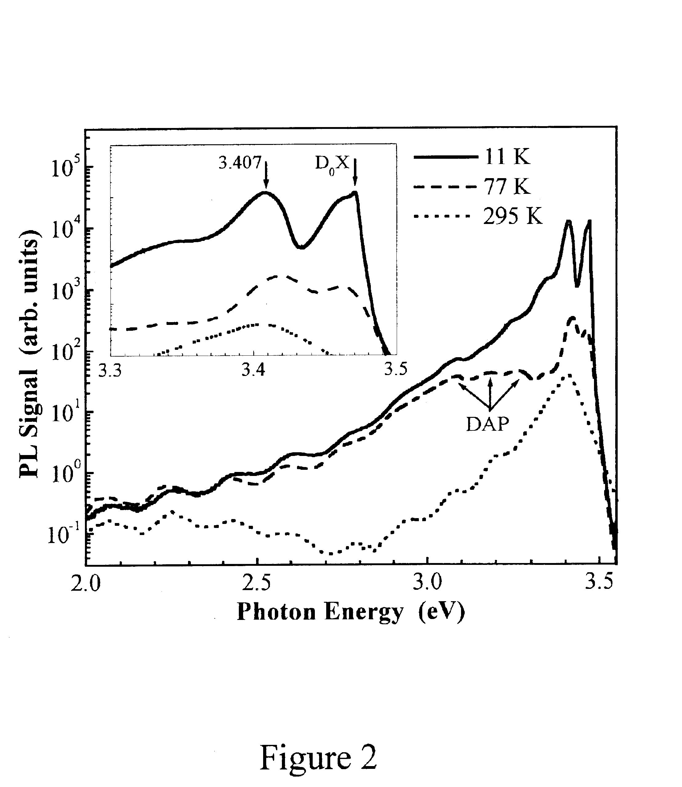
[0011]The current invention contemplates a composite wafer comprising a substrate comprising Si, a buffer layer comprising HfN overlying said Si substrate, and a GaN layer grown on said buffer layer. In another embodiment it is contemplated that there be more than one buffer layer comprising HfN, including two buffer layers touching one another. In a preferred embodiment the buffer layer of HfN has the (111) crystal structure and a layer of GaN with a wurtzite crystal polytype layer grown on said buffer layer.

[0012]Hafnium nitride has the NaCl-type structure, a lattice constant of 0.452 nm, and a mismatch of only +0.35% for GaN(0001) / HfN(111). It is a refractory metal and has been studied as a diffusion barrier in Si technology. Due to the small (0.02%) mismatch for the coincident-site lattice involving 6 HfN unit cells and 5 Si unit cells, HfN can be grown epitaxially on Si, see S. Shinkai and K. Sasaki, Jpn. J. Appl. Phys. Part 1 38, 2097 (1999), the contents of which are hereby i...


PUM

PropertyMeasurementUnit
Lengthaaaaaaaaaa

Abstract

Gallium nitride is grown by plasma-assisted molecular-beam epitaxy on (111) and (001) silicon substrates using hafnium nitride buffer layers. Wurtzite GaN epitaxial layers are obtained on both the (111) and (001) HfN/Si surfaces, with crack-free thickness up to 1.2 m. However, growth on the (001) surface results in nearly stress-free films, suggesting that much thicker crack-free layers could be obtained.

Description

PRIORITY[0001]This application claims priority to U.S. Ser. No. 60 / 381,388, filed May 17, 2002, the contents of which are hereby incorporated by reference in their entirety.STATEMENT REGARDING FEDERALLY SPONSORED RESEARCH OR DEVELOPMENT[0002]This invention was made with government support under Grant (Contract) No. DE-AC03-76F00098 awarded by The United States Department of Energy to The Regents of the University of California. The government has certain rights to this invention.BACKGROUND OF THE INVENTION[0003]Recently, there has been enormous interest in growth of Group III nitride, and particularly gallium nitride (GaN) thin films, Jpn. J. Appl. Phys. Vol. 34 (1995) pp. L 797-L 799. GaN, and related (Aluminum, Indium)N alloys are being utilized for the production of efficient optoelectronic devices, e.g. light emitters and detectors spanning the spectral range of visible to deep ultra-violet (UV). In addition, the direct wide bandgap and the chemical stability of Group III nitrid...

Claims


Application Information

Patent Timeline
IPC IPC(8): C30B23/02H01L21/02H01L21/20
CPCC30B23/02H01L21/02381H01L21/02439H01L21/02516H01L21/0254C30B29/38Y10T428/12542Y10T428/12576
Inventor ARMITAGE, ROBERT D.WEBER, EICKE R.
Owner RGT UNIV OF CALIFORNIA
Why Eureka
Try Eureka