Display device having an improved voltage level converter circuit

a voltage level converter and display device technology, applied in logic circuit coupling/interface arrangement, instruments, pulse techniques, etc., can solve the problems of low output signal level and sometimes insufficient output signal for driving pixels, and achieve the effect of increasing through current and reducing current supply capability

Inactive Publication Date: 2005-08-16
PANASONIC LIQUID CRYSTAL DISPLAY CO LTD +1
View PDF10 Cites 30 Cited by
  • Summary
  • Abstract
  • Description
  • Claims
  • Application Information

AI Technical Summary

Benefits of technology

[0009]When the voltage level converter is composed of polysilicon MOS transistors, it has been pointed out that its current supply capability is decreased further when it is gate-controlled with an external small-voltage input pulse because charge-carrier mobility in the polysilico

Problems solved by technology

These circuits are composed of transistors made of polycrystalline silicon, therefore their output signal leve

Method used


Image

  • Display device having an improved voltage level converter circuit
  • Display device having an improved voltage level converter circuit
  • Display device having an improved voltage level converter circuit

Examples


embodiment 1

[0037

[0038]Overall Configuration

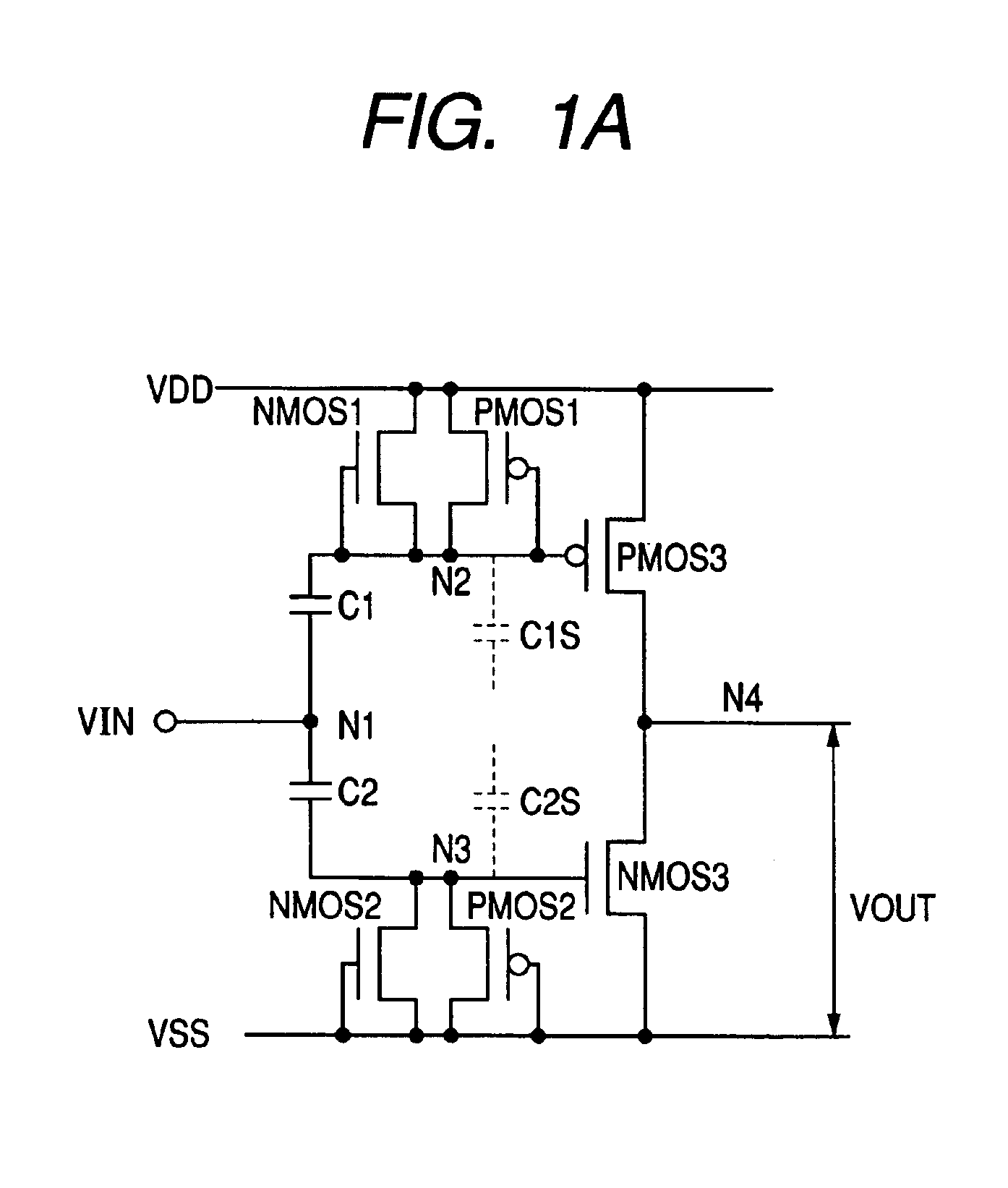
[0039]FIG. 2 is a schematic illustration of an overall configuration of the liquid crystal display device in accordance with the present invention, and is a plan view representing an actual geometrical arrangement of the components of the liquid crystal display device.

[0040]FIG. 2 depicts a transparent substrate SUB1 made of glass, for example, which is one of a pair of opposing transparent substrates sandwiching a liquid crystal layer. In a central area (a display area AR) on a liquid-crystal-layer-side surface of the transparent substrate SUB1, excluding its periphery, there are a plurality of gate signal lines GL extending in the x direction and arranged in the y direction and a plurality of drain signal lines DL extending in the y direction and arranged in the x direction.

[0041]Each pixel area is formed by an area surrounded by two adjacent gate signal lines GL and two adjacent drain signal lines DL. Each pixel area is provided with a thin film tr...

embodiment 2

[0104

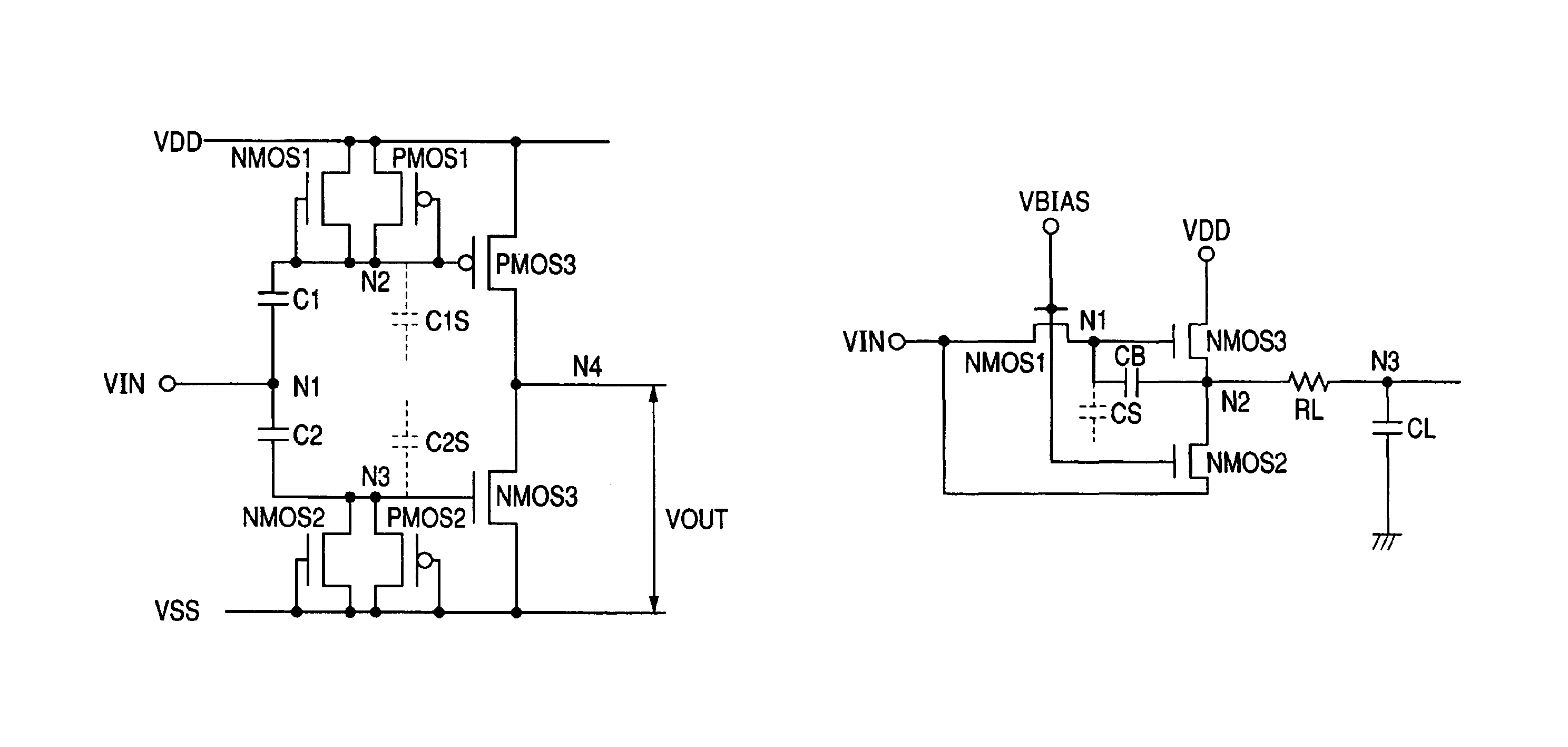
[0105]FIG. 3 is a circuit diagram of another embodiment of a voltage level converter VLC fabricated in the liquid crystal display device in accordance with the present invention. The configuration of FIG. 3 is similar to that of FIG. 1A, except that a capacitance CL is connected between the output terminal and the low-voltage power supply line VSS. The operation of this configuration is approximately the same in performance as that of FIG. 1A.

[0106]Here, in the operation of the circuit of FIG. 1A, for simplicity, VINT is replaced with VDD in the inequality (9). The inequality (9) is assumed to be a condition for making V(N4) equal to VSS, and the inequality (16) is assumed to be a condition for making V(N4) equal to VDD.

[0107]First, the following inequalities (20) and (21) are obtained from the inequalities (9) and (16), respectively:

I(NMOS3, Vth(PMOS2))×(t2−t1)≧{C(N4)+CL}×(VDD−VSS)  (20),

I(PMOS3, Vth(PMOS1))×(t3−t2)≧{C(N4)+CL}×(VDD−VSS)  (21).

[0108]Solving these inequalities (...

embodiment 3

[0116

[0117]FIG. 5 is a circuit diagram of another embodiment of the voltage level converter VLC in accordance with the present invention, and is similar to that of FIG. 3.

[0118]The circuit diagram of FIG. 5 differs from that of FIG. 4A in that another stage of the CMOS is added which is composed of a p-channel type MOS transistor PMOS5 and an n-channel type MOS transistor NMOS5, and the load capacitance CL is coupled between its output terminal and the low-voltage power supply line VSS. In FIG. 5, reference character C5 denotes a parasitic capacitance such as a wiring capacitance at the node N5, and a node N6 forms the output terminal. The voltage level converter of this configuration is advantageous in the case of a large load capacitance.

[0119]It is needles to say that, to enhance the beneficial effects of this embodiment further, still another stage of the CMOS may be added which is composed of a p-channel type MOS transistor PMOS6 and an n-channel type MOS transistor NMOS6, and ...


PUM


Abstract

A display device has a driver including a level converter formed of polysilicon MISTFTs. The level converter includes first, second and third N-channel MISTFTs (NMISTFTs) and first, second and third P-channel MISTFTs (PMISTFTs). Gate and first terminals of the first NMISTFT and PMISTFT, and a gate terminal of the third PMISTFT are coupled to an input terminal via a capacitance. Second terminals of the second NMISTFT and PMISTFT, and a gate terminal of third NMISTFT are coupled to the input terminal via a capacitance. A first terminal of the third PMISTFT, and second terminals of the first NMISTFT and PMISTFT are coupled to a high voltage. A second terminal of the third NMISTFT, gate and first terminals of the second NMISTFT and PMISTFT are coupled to a low voltage. A second terminal of the third PMISTFT and a first terminal of the third NMISTFT are connected to an output terminal.

Description

CROSS REFERENCE TO RELATED APPLICATIONS[0001]This application is a Continuation application of application Ser. No. 09 / 988,209, filed Nov. 19, 2001 now U.S. Pat. No. 6,686,899, the entire disclosure of which is hereby incorporated by reference.BACKGROUND OF THE INVENTION[0002]The present invention relates to a display device, and in particular to an active matrix type display device having a driver circuit for driving pixels, fabricated on its substrate of its display panel.[0003]A display panel has an electrooptical material layer sandwiched between a pair of substrates. In this specification, the term “electrooptical material” refers to material which changes its optical properties such as transmission, emission, refractive index and absorption of light under the influence of an electric field or current. The electrooptical material includes liquid crystal material and electroluminescent material, for example.[0004]By way of example, an active matrix type liquid crystal display de...

Claims


Application Information

Patent Timeline
IPC IPC(8): G09G3/36G02F1/136G02F1/133G09G3/20G09G3/26G09G3/30H03K5/003H03K19/00H03K19/0185
CPCG09G3/3648H03K5/003H03K19/0013H03K19/018571G09G2300/0408G09G2310/0289G09G2330/02G02F1/133
Inventor MIYAZAWA, TOSHIOSATOU, HIDEOSATOU, TOMOHIKOMAKI, MASAHIRO
Owner PANASONIC LIQUID CRYSTAL DISPLAY CO LTD
Why Eureka
Try Eureka