Imaging X-ray detector based on direct conversion

a detector and x-ray technology, applied in the field of direct conversion of x-ray detectors, can solve the problems of reducing the efficiency of collecting information from objects under study, introducing noise, and introducing such a structure with good yield and high homogenous gain throughout the detecting surface, and achieves the effect of high yield and high homogenous gain

Inactive Publication Date: 2005-08-23
OXFORD INSTUMENTS ANALYTICAL LIMITED +1
View PDF7 Cites 32 Cited by
  • Summary
  • Abstract
  • Description
  • Claims
  • Application Information

AI Technical Summary

Benefits of technology

[0017]The advantageousness of combining just GaAs with Ge comes from the near sameness of certain lattice constants of the two materials. Close lattice constants mean that producing a nice and regularly grown epitaxial layer of one material on top of the other in the manufacturing process is easy. Additionally recombination at the material interface can be made negligible. The high purity of the Ge layer means that the detection response of the detector can be made extremely homogenous throughout the detector area.

Problems solved by technology

The drawbacks of the conventional approach arise from the large number of different devices and components that take part in converting the spatial distribution of differently attenuated x-rays into an actual image.
Taking the signal through a variety of devices and components reduces the efficiency of collecting information from the object under study and introduces noise.
However, producing such a structure with good yield and highly homogenous gain throughout the detecting surface may be problematic.
Another disadvantage of the structure of FIG. 3 are that only approximately one half of the visible light photons can be collected.
The drawbacks of the Se-based direct conversion detector arrangements have been associated with questionable reliability as well as a relatively low DQE (Detective Quantum Efficiency) values, which cause degradation to image quality and preclude the use of Se-based direct conversion detectors in advanced applications of X-ray diagnostics and therapy.

Method used


Image

  • Imaging X-ray detector based on direct conversion
  • Imaging X-ray detector based on direct conversion
  • Imaging X-ray detector based on direct conversion

Examples


Embodiment Construction

[0030]The exemplary embodiments of the invention presented in this patent application are not to be interpreted to pose limitations to the applicability of the appended claims. The verb “to comprise” is used in this patent application as an open limitation that does not exclude the existence of also unrecited features. The features recited in depending claims are mutually freely combinable unless otherwise explicitly stated.

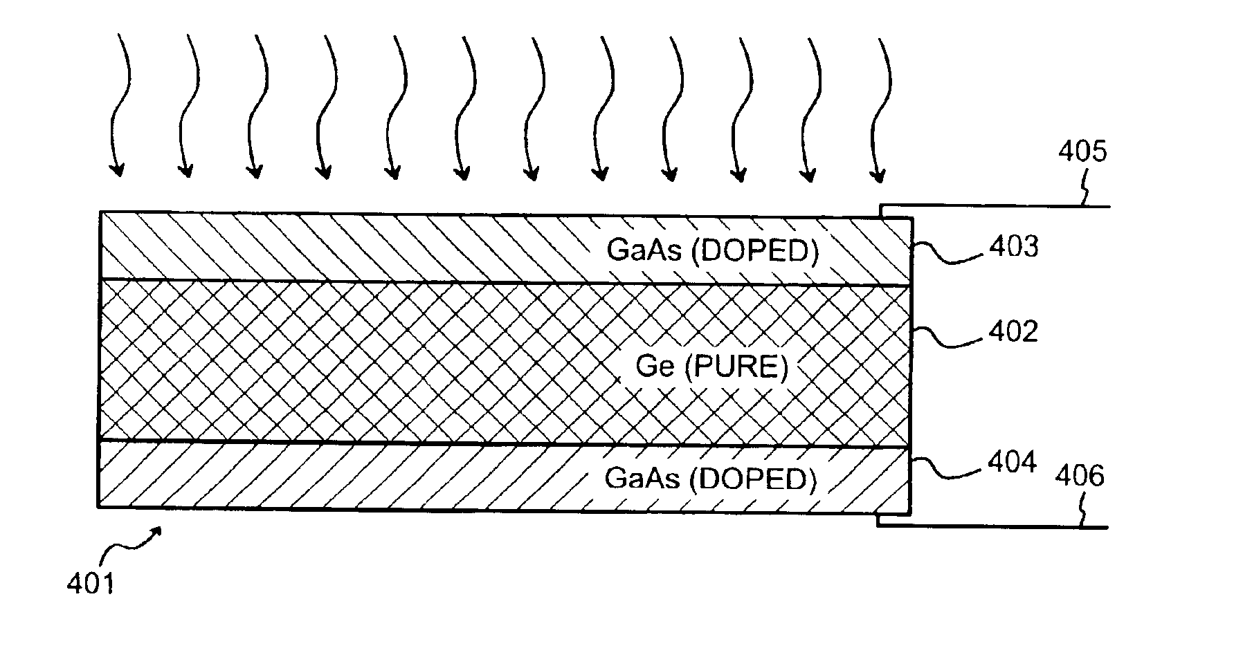
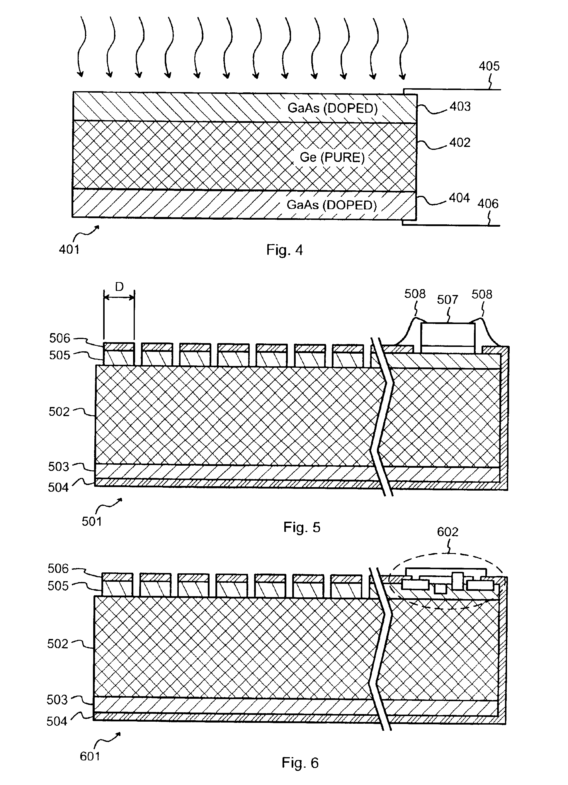
[0031]FIG. 4 is a schematic cross section through a stack of semiconductor layers that together constitute the radiation-sensitive parts of an X-ray detector 401. Basically the detector's semiconductor stack consists of a pure Ge layer 402 sandwiched between two oppositely doped GaAs layers 403 and 404. “Oppositely doped” means that one of the GaAs layers 403 and 404 is an n-type semiconductor layer and comprises a surplus of negative charge carriers (electrons), while the other is a p-type semiconductor layer and comprises a surplus of positive charge carriers (...


PUM

PropertyMeasurementUnit
thicknessaaaaaaaaaa
thicknessaaaaaaaaaa
thicknessaaaaaaaaaa

Abstract

An X-ray detector (401, 501, 601) has a detecting element that comprises a semiconductor heterostructure where an undoped Germanium layer (402, 502) is enclosed between two oppositely doped Gallium Arsenide layers (403, 404, 503, 505).

Description

TECHNICAL FIELD[0001]The invention concerns generally the technology of producing digital images of objects illuminated with X-rays. Especially the invention concerns the composition, structure and manufacturing method of a detector that is used for producing a digital image of the illuminated object.BACKGROUND OF THE INVENTION[0002]FIG. 1 illustrates schematically a conventional way of producing an X-ray image in electronic form. An X-ray tube 101 emits X-rays that propagate through an object under study (such as a part of a human body) 102 and enter an image intensifier 103. Optical equipment 104 convey the output signal of the image intensifier 103 onto a CCD array 105, from which the two-dimensional image is read and stored into a memory 106 and / or shown on a display 107. The drawbacks of the conventional approach arise from the large number of different devices and components that take part in converting the spatial distribution of differently attenuated x-rays into an actual i...

Claims


Application Information

Patent Timeline
Patent Type & Authority Patents(United States)
IPC IPC(8): G01N23/02G01N23/04G01T1/24G01T1/00G21K5/02H01L27/14H01L31/08H01L31/09H04N5/32G01TG01T1/20H01L31/0264H01L31/105
CPCG01T1/2018H01L27/14659H01L31/0264H01L31/105G01T1/241
Inventor SIPILA, HEIKKI JOHANNESBOURGOIN, JACQUES
Owner OXFORD INSTUMENTS ANALYTICAL LIMITED
Why Eureka
Try Eureka