Light emitting device

a technology of light emitting device and light emitting element, which is applied in the direction of thermoelectric device, electroluminescent light source, electric lighting source, etc., can solve the problems of reducing the efficiency of actual aperture, increasing the manufacturing cost, and the process temperature of about 450° c. in the tft cannot be withstood, so as to improve the yield of color filter, prevent short circuit of light emitting element, and enhance the surface of translucent electrod

Inactive Publication Date: 2005-08-23
SEMICON ENERGY LAB CO LTD
View PDF13 Cites 25 Cited by
  • Summary
  • Abstract
  • Description
  • Claims
  • Application Information

AI Technical Summary

Benefits of technology

[0025]Moreover, the present invention can prevent the components such as pigment and the like contained in the coloring layer from diffusing to the TFT side by intervening an inorganic insulating film such as silicon nitride between the flattened film and the coloring layer. Moreover, the present invention can prevent the components such as pigment and the like contained in the coloring layer from diffusing to the light emitting element side by forming an inorganic insulating film such as silicon nitride film between this translucent electrode (anode) and the coloring layer.
[0026]Moreover, the surface of the coloring layer of color filter may be polished and flattened. By thus performing, the yield of the color filter can be enhanced and at the same time, the flatness of the surface of the translucent electrode (anode) can be enhanced, and the short circuit of the light emitting element can be prevented.
[0027]In any case, a pin hole test of the coloring layer can be carried out at this stage by forming the coloring layer of the color filter on the flattened layer, and in the case where it does not reach the predetermined standard, the coloring layer is peeled off and reprocessing can be done. As a method of peeling off, it may be washed and removed by a solvent, or it may be also mechanically polished and cutout. In any case, since the flattened film exists there, the reprocessing can be provided without damaging the TFTs.

Problems solved by technology

However, when the color filter and pixel matrix in which a light emitting element is provided in each pixel are individually formed, it is necessary to align both with a high accuracy and assemble them, and in the case where the alignment accuracy is low, there has been a problem that the actual aperture efficiency is lowered.
However, since the heat resistance temperature is about 200° C., the process temperature of about 450° C. in the TFT could not be withstood.
Moreover, a material referred to as a color resist used at the time when the colored layers of the color filters are formed is considerably expensive material, and there has been a problem that such a process in which the yield of TFT steps and color filter steps are integrated is a factor of increasing the fabricating cost and thus is not suitable.

Method used


Image

  • Light emitting device
  • Light emitting device
  • Light emitting device

Examples


Embodiment Construction

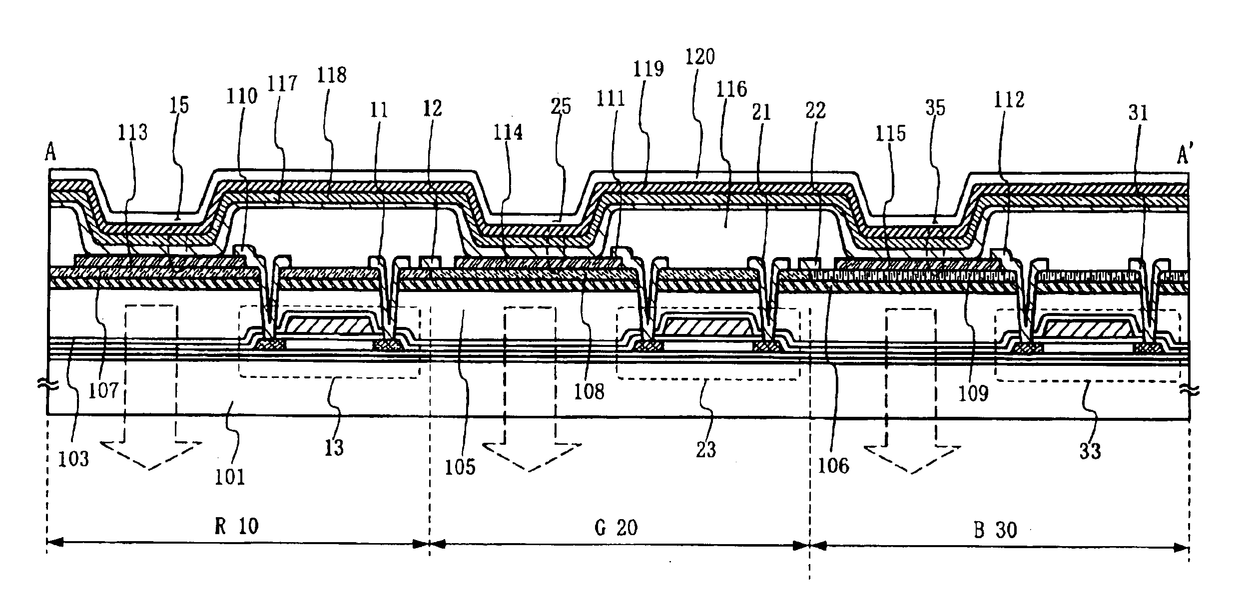
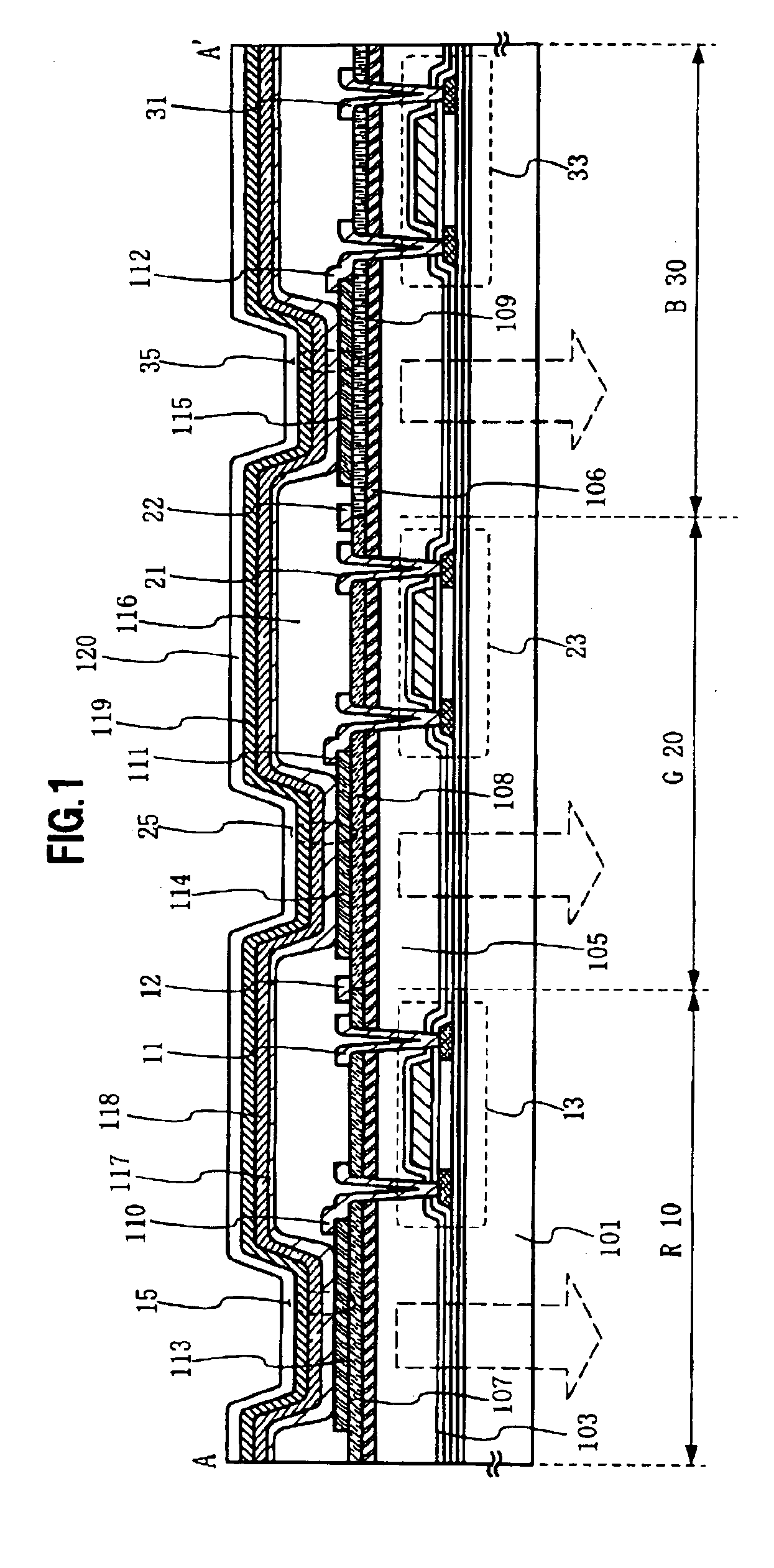
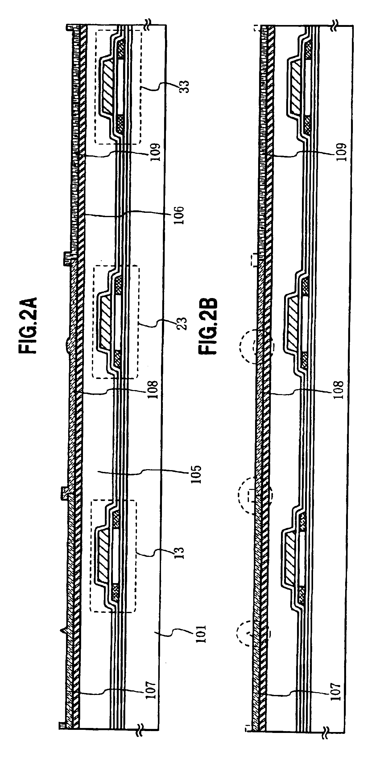
[0035]Hereinafter, Embodiments of the present invention will be described in detail with reference to the drawings. In FIG. 5, one form of a light emitting device in which a substrate 900 is equipped with a pixel section 902, gate signal side drive circuits 901a, 901b, a data signal side drive circuit 901c, an input and output terminal section 935 and a wiring or wiring group 917 is shown. A sealing pattern 940 may be partially overlapped with the gate signal line side drive circuits 901a, 901b, the data signal line side drive circuit 901c and the wiring or wiring group 917 connecting the relevant drive circuit section and an input terminal. By thus performing, the area of the frame region of the display panel (peripheral region of pixel section) can be diminished. A FPC 936 is attached to and fixed on the exterior input terminal section.

[0036]In the pixel section 902, a TFT and a light emitting element are provided per each pixel, and these are arrayed in a matrix shape and thus co...


PUM


Abstract

It is considered that in the fabricating steps of a TFT substrate, a color filter layer is prepared at the same alignment accuracy. However, since the heat resistance temperature is about 200° C., it could not withstand the process temperature of about 450° C. in the TFT. The pixel section is formed by arraying in a matrix shape a light emitting element in which an organic compound layer having the luminous property is formed between a pair of electrodes consisting of a translucent electrode and a non-translucent electrode and a TFT, the coloring layer of color filter provided corresponding to each pixel is provided in contact with the flat surface of the flattened insulating film composed of an inorganic or organic material between the light emitting element and the TFT, the boundary region of coloring layers adjacent each other is provided while overlapping with a gate signal line or data line for transmitting a signal to the TFT, and the translucent electrode is provided while overlapping with the layer inside of the coloring layer.

Description

BACKGROUND OF THE INVENTION[0001]1. Field of the Invention[0002]The present invention relates to a method of preparing a light emitting device equipped with a light emitting element having a layer composed of an organic compound (hereinafter, referred to as organic compound layer), and particularly relates to a multi-color display function.[0003]2. Prior Art[0004]Since a spontaneous emission type display device using a light emitting element in which an organic compound layer is intervened between a pair of electrodes has a wide angular field of view and is also excellent in visibility, it has drawn the attention as a display device of the next generation.[0005]A light emitting mechanism of a light emitting element is considered as the phenomenon that a hole injected from an anode which is one of a pair of electrodes and an electron injected from a cathode which is the other one of a pair of electrodes recombine in a luminescent organic compound layer (light emitting layer) and form...

Claims


Application Information

Patent Timeline
Patent Type & Authority Patents(United States)
IPC IPC(8): H01L27/32H01L27/28
CPCH01L27/322H01L27/3258H10K59/38H10K59/124H05B33/00
Inventor YAMAZAKI, SHUNPEI
Owner SEMICON ENERGY LAB CO LTD
Why Eureka
Try Eureka