Method of removing metal etching residues following a metal etchback process to improve a CMP process

a metal etching and cmp technology, applied in the field of metal etching residue removal following a metal etching back process, can solve the problems of process wafer surface scratching, method failure, and inability to reduce the level of scratching, and achieve the effect of reducing the scratching level of the wafer surfa

Inactive Publication Date: 2005-08-30
TAIWAN SEMICON MFG CO LTD
View PDF7 Cites 106 Cited by
  • Summary
  • Abstract
  • Description
  • Claims
  • Application Information

AI Technical Summary

Benefits of technology

[0007]To achieve the foregoing and other objects, and in accordance with the purposes of the present invention, as embodied and broadly described herein, the present invention provides a method for reducing wafer surface scratching in a metal CMP process.

Problems solved by technology

A serious problem in tungsten plug formation according to prior art methods of using a dry etchback process to remove the tungsten metal above the via level is that during the dry etchback process residual metal containing particles ranging in size from about 0.5 microns to about 40 microns frequently remain on the wafer process surface.
A major problem in tungsten plug formation process is the scratching of the process wafer surface caused by the residual particles or etching residue in a subsequent CMP process.
These methods have not been entirely successful and have been found in many cases to fail to reduce the level of scratching in subsequent CMP processes.

Method used


Image

  • Method of removing metal etching residues following a metal etchback process to improve a CMP process
  • Method of removing metal etching residues following a metal etchback process to improve a CMP process
  • Method of removing metal etching residues following a metal etchback process to improve a CMP process

Examples


Embodiment Construction

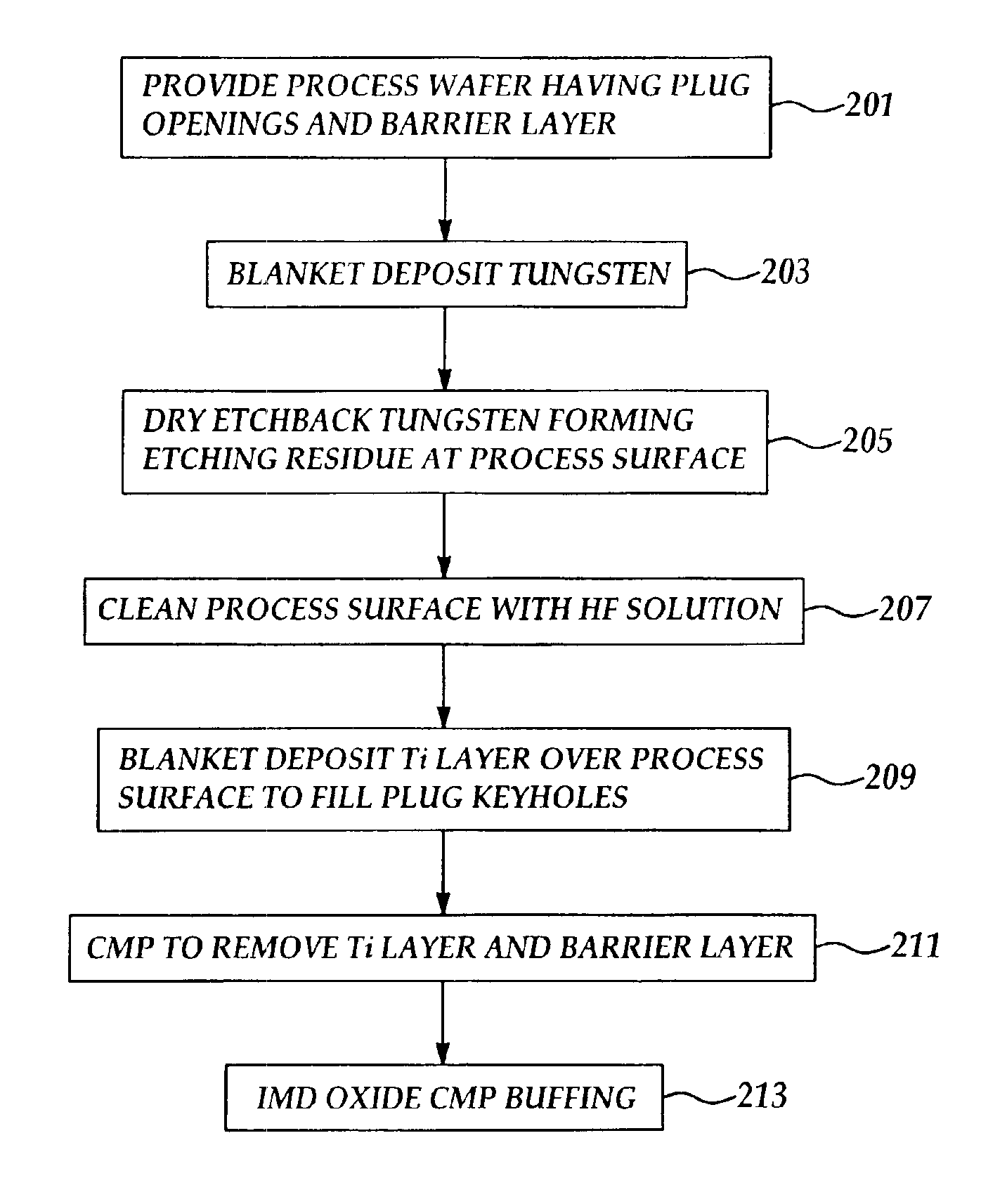
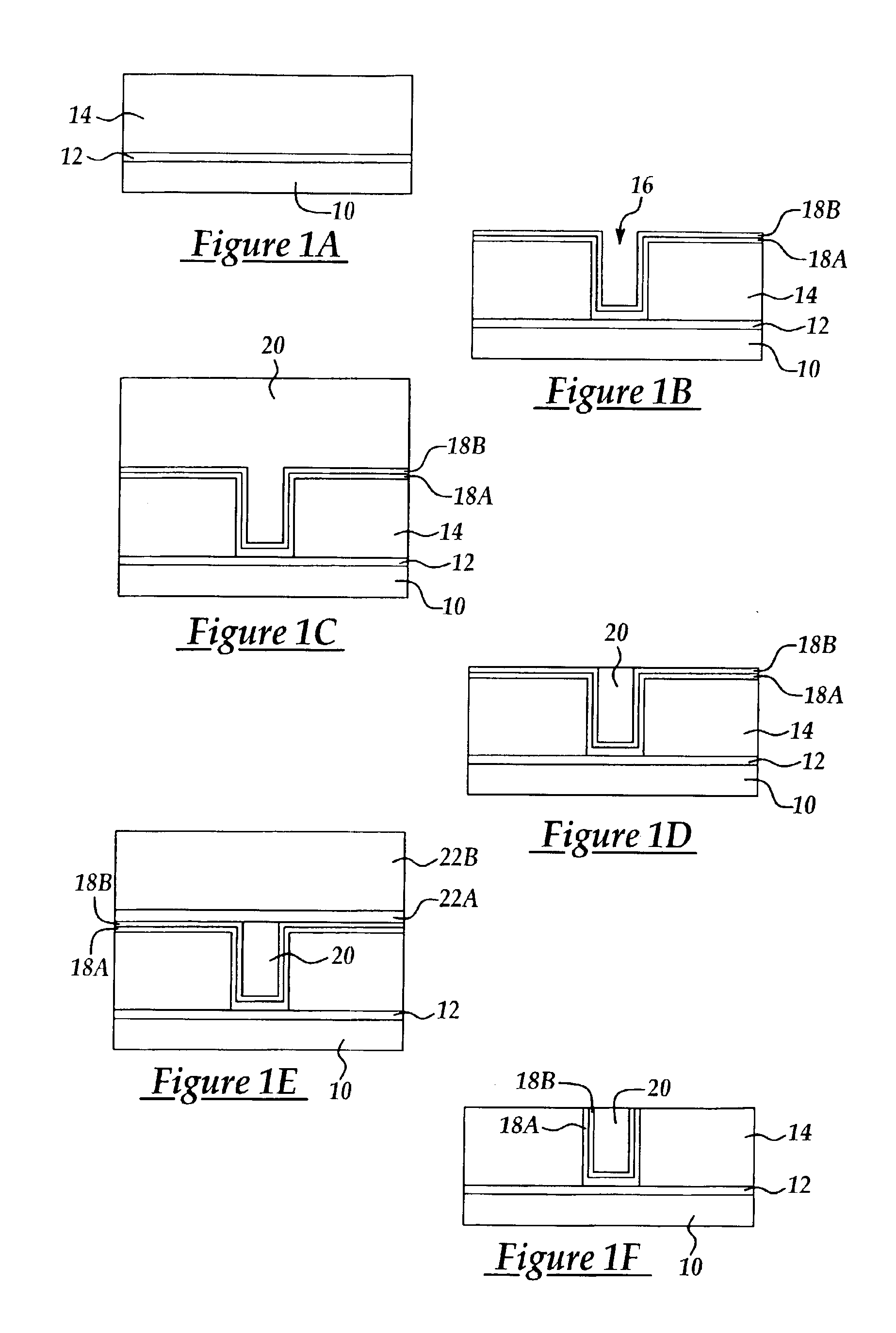
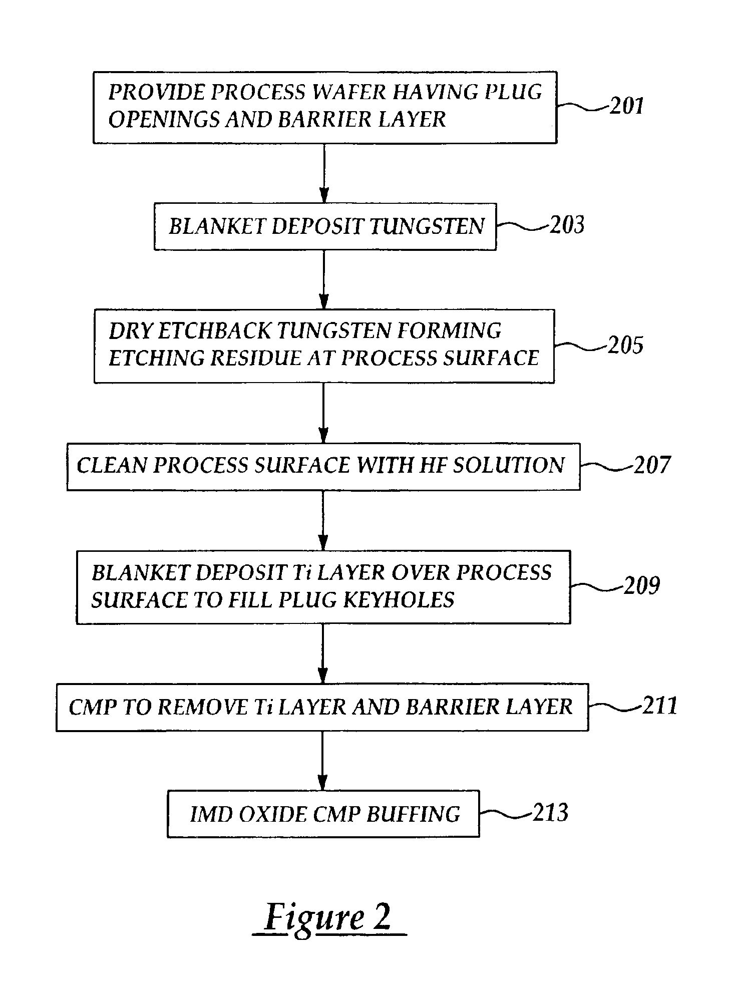
[0012]Although the method of the present invention is explained by reference to formation of a tungsten plug, it will be appreciated that the method of the present invention may be advantageously applied to any metal plug formation process where residual metallic contaminates form on a process surface whereby components in the etching chemistry have chemically reacted with a metal layer in a dry etchback process to produce a metal containing etching by-product at the process surface.

[0013]In a first embodiment, the method includes providing a semiconductor wafer including a dielectric insulating layer having plug openings lined with a barrier layer formed according to a blanket deposition process and an overlying first metal layer formed according to a blanket deposition process filling the plug openings; dry etching in an etchback process to remove at least a portion of the first metal layer above the plug opening level while forming a metallic etching residue by reaction with an e...


PUM

PropertyMeasurementUnit
thicknessaaaaaaaaaa
sizeaaaaaaaaaa
thicknessaaaaaaaaaa

Abstract

A method for reducing wafer surface scratching in a metal CMP process including providing a semiconductor wafer having a process surface comprising a blanket deposited metal layer; dry etching in an etchback process comprising a fluorine containing etching chemistry to remove at least a portion of the metal layer forming a metal and fluorine containing etching residue at the process surface; cleaning the process surface with a hydrofluoric acid (HF) containing cleaning solution; and carrying out a subsequent metal chemical mechanical polishing (CMP) process.

Description

FIELD OF THE INVENTION[0001]This invention generally relates to semiconductor processing methods including formation of metallization plugs and more particularly to a method to reduce CMP scratching caused by metallic residue contamination formed during a metal etchback process.BACKGROUND OF THE INVENTION[0002]Metallization interconnects are critical to the proper electronic function of semiconductor devices. Several advances in semiconductor processing have been aimed at improving signal transport speed by reducing metal interconnect resistivities and improving resistance to electromigration effects. Copper has increasingly become a metal of choice in, for example, upper levels of metallization in a multi-level semiconductor device due to its low resistivity and higher resistance to electromigration. Tungsten is still preferred for use in the lower metallization layers adjacent to the silicon substrate since it provides an effective diffusion barrier to metal diffusion from overlyi...

Claims


Application Information

Patent Timeline
Patent Type & Authority Patents(United States)
IPC IPC(8): H01L21/02H01L21/70H01L21/768H01L21/3213H01L21/321H01L21/3105
CPCH01L21/02074H01L21/31053H01L21/32115H01L21/3212H01L21/76877
Inventor HUANG, YAI-YEIFAN, YUH-DA
Owner TAIWAN SEMICON MFG CO LTD
Why Eureka
Try Eureka