

Semiconductor device having a gate wiring comprising laminated wirings
a technology of laminated wiring and semiconductor devices, which is applied in the field of semiconductor devices, can solve the problems of reducing the accumulated capacity of capacitors, lowering the contrast of image displays, and high off currents, and achieves the effect of improving the operation performance and reliability of semiconductor devices
- Summary
- Abstract
- Description
- Claims
- Application Information
AI Technical Summary
Benefits of technology
Problems solved by technology
Method used
Image

Examples
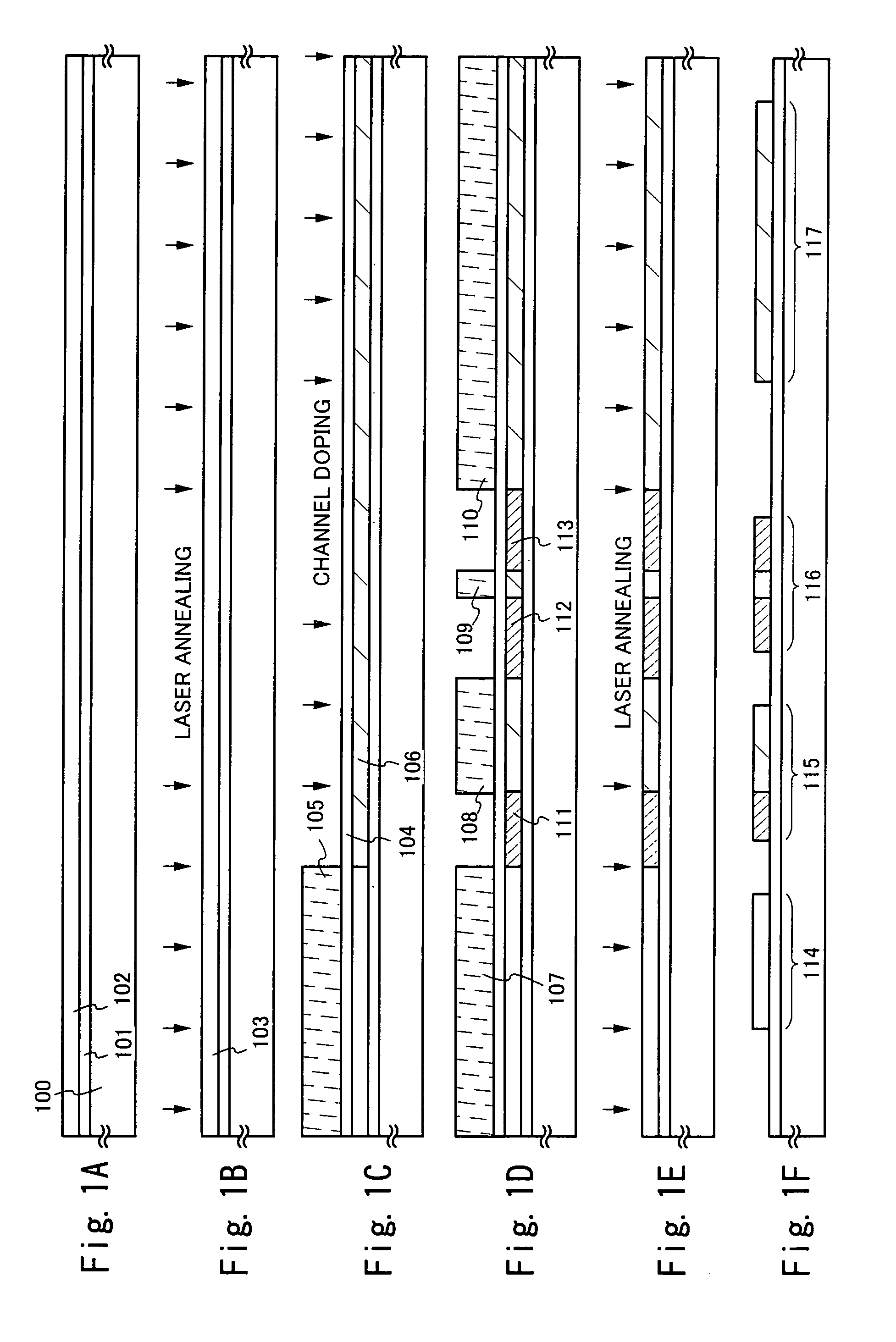
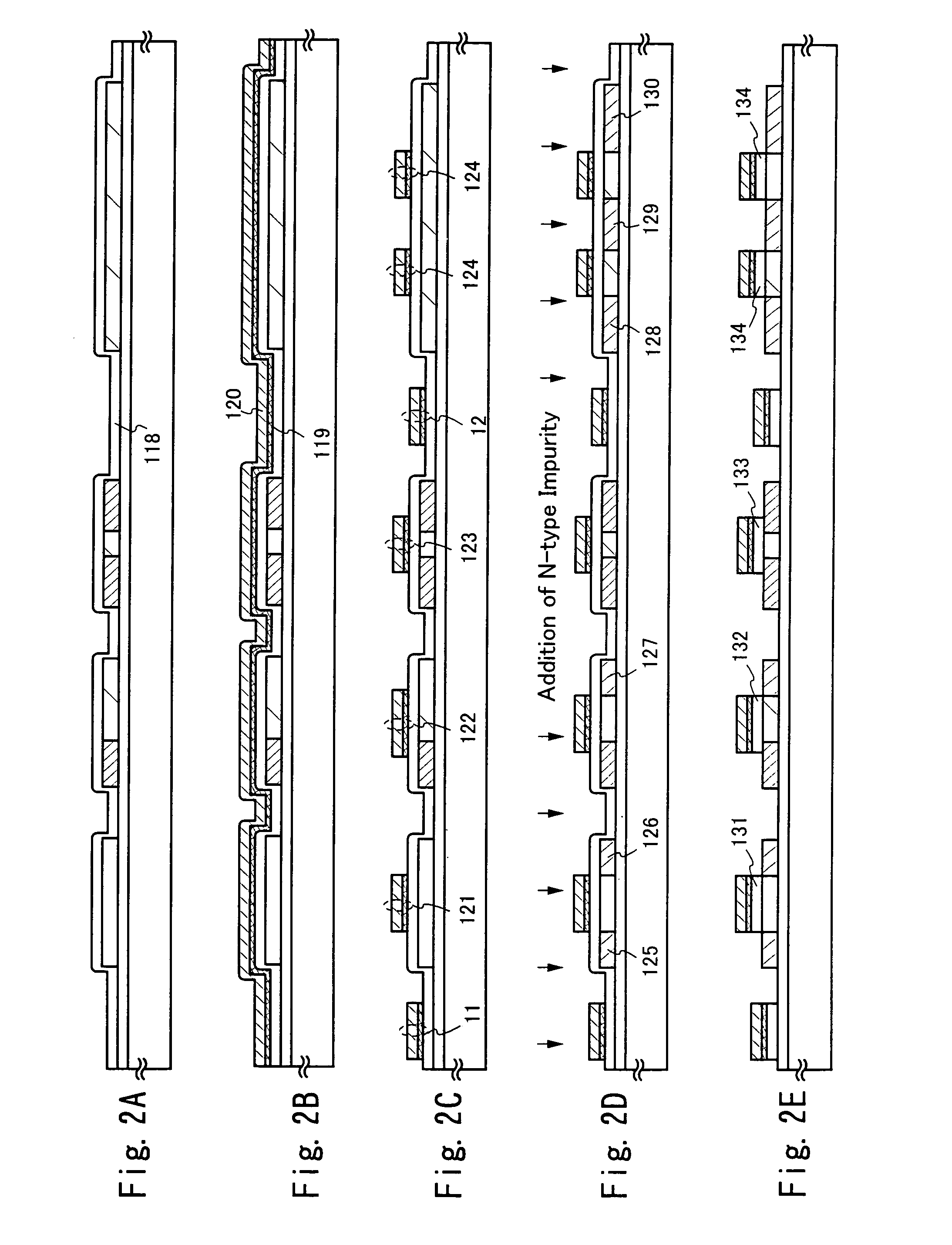
embodiment 1
[0063]An embodiment according to the present invention is described by using FIGS. 1A to 4B. Here a method for fabricating TFTs of a pixel section and a driver circuit provided in its peripheral, at the same time, is described. Provided, for the simplicity of explanation, a CMOS circuit which is a basic circuit for a shift register and buffer etc., and an n-channel TFT forming a sampling circuit are shown for the driver circuit.
[0064]In FIG. 1A, it is preferable to use a glass substrate or a quartz substrate for substrate 100. A silicon substrate, a metal substrate or a stainless substrate having an insulating film formed on the surface thereof can be used, too. If heat resistivity permits, plastic substrate may also be used.
[0065]A base film 101 that comprises a silicon-containing insulating film (the term “insulating film” generically represents a silicon oxide film, a silicon nitride film and a silicon nitride oxide film in this specification) is formed by plasma CVD or sputterin...
embodiment 2
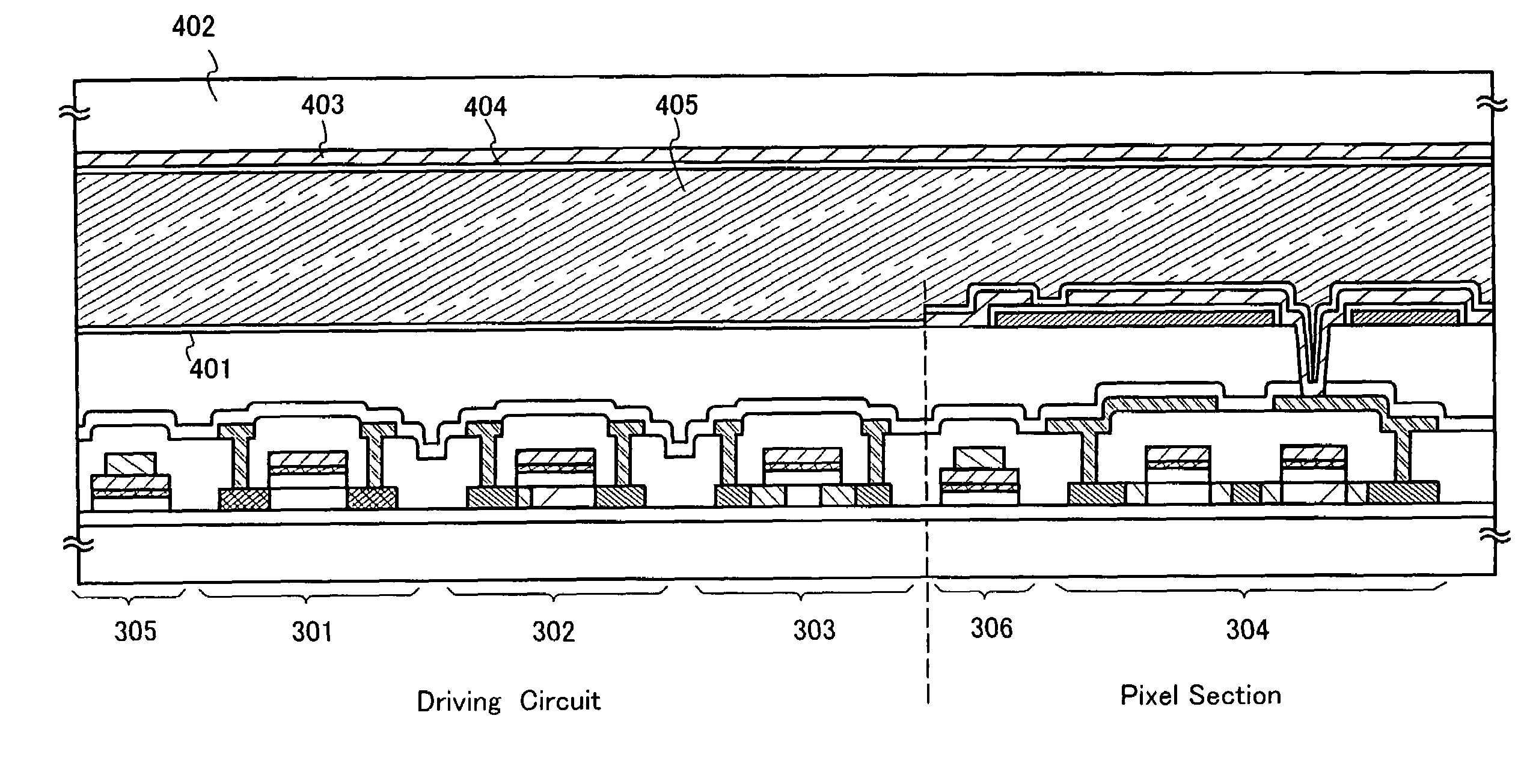
[0153]A process of manufacturing an active matrix type liquid crystal display device from an active matrix substrate is next explained. As shown in FIG. 5, an alignment film 401 is formed for the substrate in the state of FIG. 4B. In the present embodiment, a polyimide film is used for the alignment film. An opposing electrode 403 comprising transparent conductive film and an alignment film 404 are formed on an opposing substrate 402. Color filter or a shielding film may be formed on the opposing substrate if necessary.
[0154]After forming the alignment films, a rubbing process is performed to give the liquid crystal molecules a certain fixed pre-tilt angle, so that they are aligned. The active matrix substrate, on which a pixel circuit and driver circuits are formed, and the opposing substrate are stuck together through a sealing material, spacers, or a resin film provided by patterning (not shown in the figures) in accordance with a known cell assembly process. A liquid crystal mat...
embodiment 3
[0156]FIG. 8 shows an example of circuit structure of the active matrix substrate shown in embodiment 2. The active matrix substrate of embodiment 3 has a image signal driver circuit 801, a scanning signal driver circuit (A) 807, a scanning signal driver circuit (B) 811, a pre-charge circuit 812, and a pixel section 806. Through the Specification, driver circuit is a generic name including image signal driver circuit 801 and a scanning signal driver circuit 807.
[0157]The image signal driver circuit 801 is provided with a shift register 802, a level shifter 803, a buffer 804, and a sampling circuit 805. Further, the scanning signal driver circuit (A) 807 is provided with a shift register 808, a level shifter 809, and a buffer 810. The scanning signal driver circuit (B) 811 has a similar structure.
[0158]The driver voltages for the shift register 802 and 808 is between 5 and 16 V here (typically 10 V), and the structure shown by reference numeral 302 in FIG. 4B is suitable for n-channe...
PUM
 Abstract
Description
Claims
Application Information