Semiconductor integrated circuit

a technology of integrated circuits and semiconductors, applied in the direction of logic circuits characterised by logic functions, pulse techniques, electronic switching, etc., can solve the problems of thermal runaway, device characteristics are deteriorated, potential fluctuation, etc., to prevent the area of the chip from increasing, and to effectively use available space

Inactive Publication Date: 2005-08-30
RENESAS ELECTRONICS CORP
View PDF13 Cites 8 Cited by
  • Summary
  • Abstract
  • Description
  • Claims
  • Application Information

AI Technical Summary

Benefits of technology

[0011]It is an object of the present invention to provide a high-performance CMOS semiconductor integrated circuit which is capable of preventing the latch-up phenomenon, and its fabrication method.
[0012]Moreover, it is another object of the present invention to provide a way of preventing the latch-up phenomenon of a CMOS semiconductor integrated circuit from occurring under normal operation of the semiconductor integrated circuit and of preventing a leakage current from being generated during a test of the circuit.
[0013]Furthermore, it is still another object of the present invention to provide a way of improving the reliability of a CMOS semiconductor integrated circuit under normal operation and under test, without lowering the operation speed of the semiconductor integrated circuit under normal operation of the circuit. Furthermore, it is still another object of the present invention to provide a way of improving the reliability of a CMOS semiconductor integrated circuit under the normal operation and test of the circuit without deteriorating the device characteristics.

Problems solved by technology

However, because lowering of the threshold voltage causes an increase in leakage current, a leakage current test (I ddq test) widely used for testing a semiconductor integrated circuit cannot be performed, and, moreover, in the case of an aging test, the temperature is excessively raised due to an increase in the leakage current and, thereby, a problem of thermal runaway occurs
By applying a back bias to the well of a MOS FET in order to solve the above problem, it is possible to control the threshold voltage In the case of this technique, however, the well potential may fluctuate due to noise under practical use (under normal operation) and a problem may occur in which a forward current is applied between the well and the source / drain to produce a so-called latch-up phenomenon.
Therefore, problems occur in that (1) it is necessary to generate a voltage higher than the power supply voltage under normal operation, and (2) the device characteristics are deteriorated because the high voltage in the above Item (1) is applied to the MOS FET and, thereby, the thickness of the gate oxide film of the MOS FET must be increased

Method used


Image

  • Semiconductor integrated circuit
  • Semiconductor integrated circuit
  • Semiconductor integrated circuit

Examples


Embodiment Construction

[0078]The present invention will be described herein in detail with reference to the accompanying drawings. In all drawings for explaining the various embodiments, components having the same function are provided with the same symbol and a repetitive explanation thereof will be omitted.

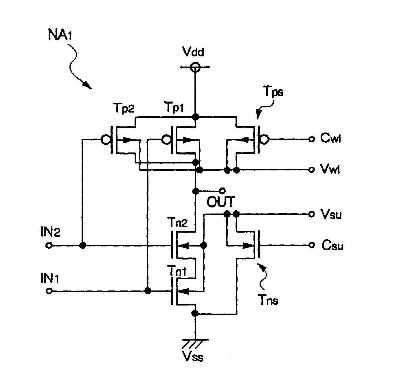
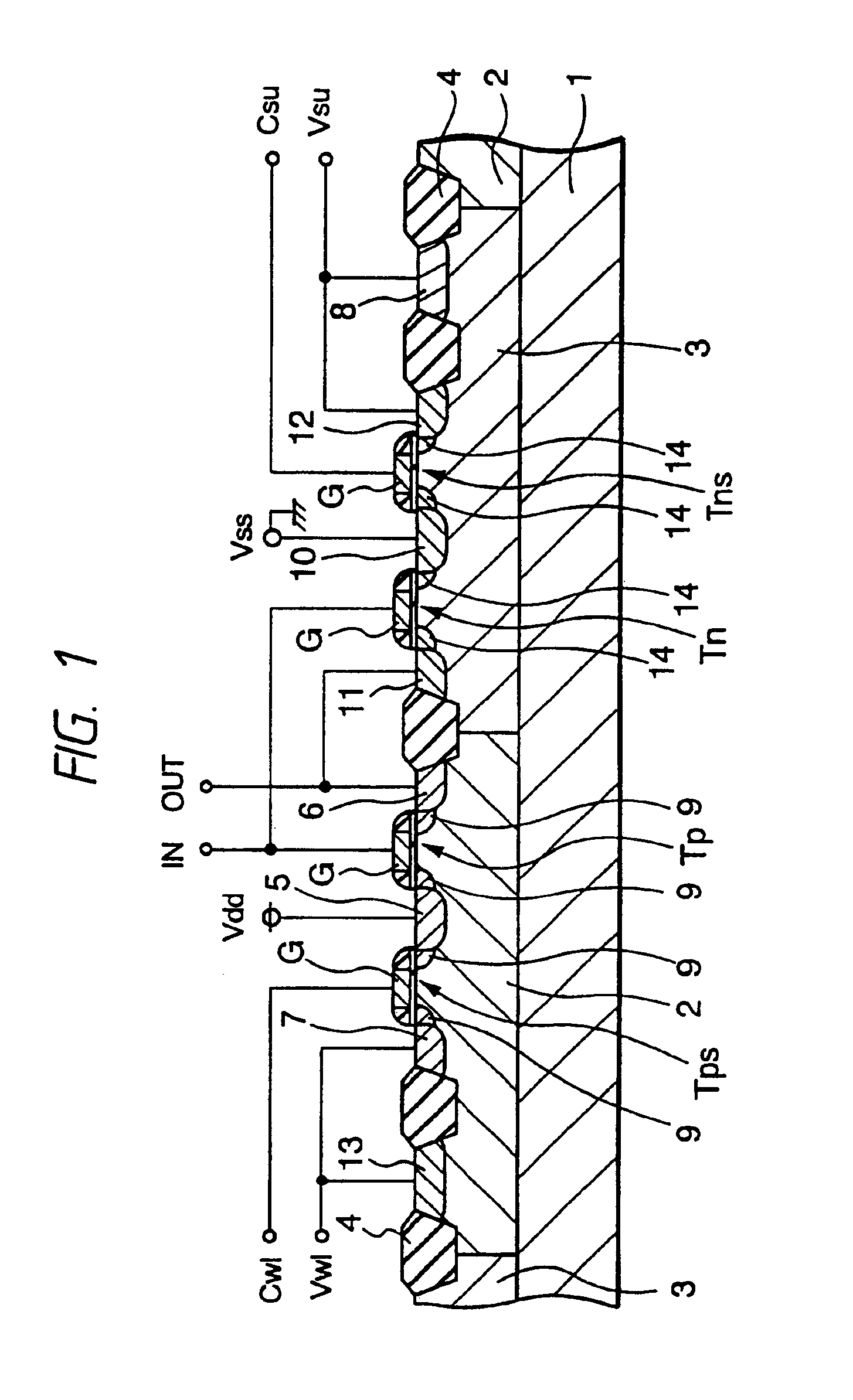
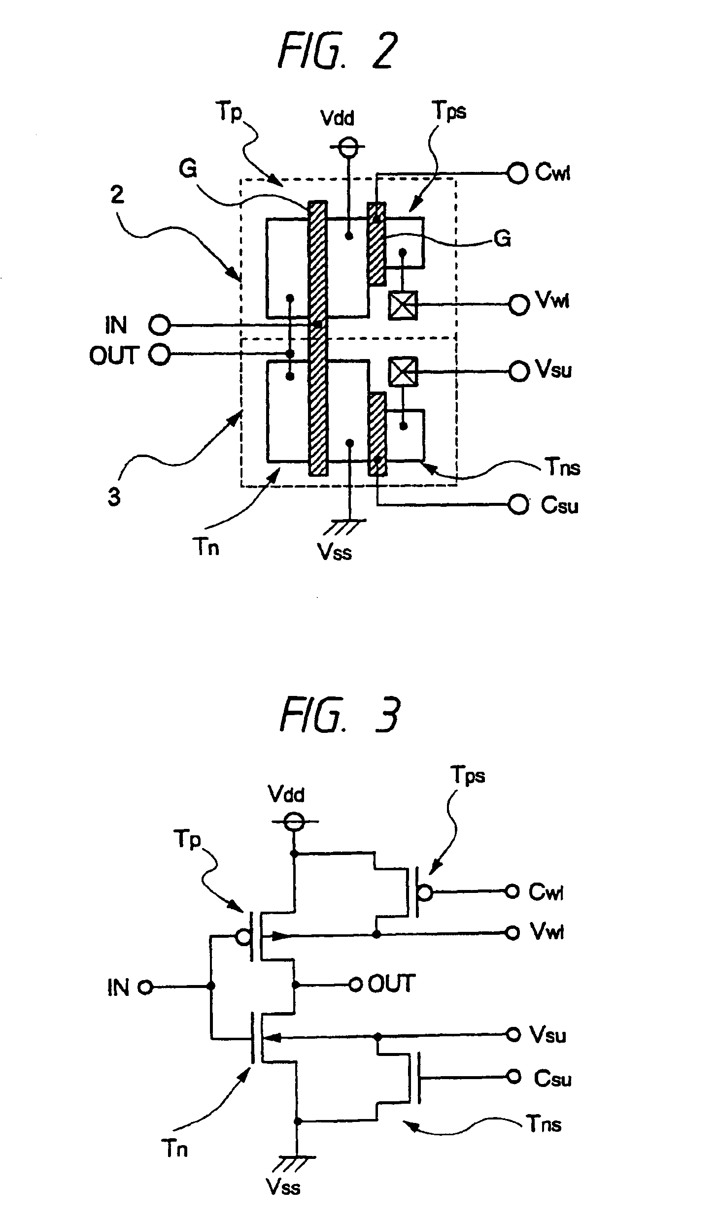
[0079]The CMOS semiconductor integrated circuit of a first embodiment will be specifically described while referring to FIGS. 1 to 5. FIGS. 1 to 3 show the region of an inverter used for the logic gate of a CMOS semiconductor integrated circuit.

[0080]Moreover, in this specification, a symbol such as Vdd is used to represent a voltage as a general indication, as well as to represent a wiring to which the voltage is applied. Moreover, in FIGS. 1 to 3, a circular mark denotes an electrode, such as a pin, provided for an end of each wiring, and a square provided with hatching x denotes a contact region connecting different wiring layers, that is, the region of a through-hole conductive layer embedded in a...


PUM


Abstract

An integrated circuit having a CMOS circuit constituted by electrically connecting an n-type well 2, in which p-channel transistor Tp of the CMOS circuit is set, with a supply line Vdd through switching transistor Tps, and electrically connecting a p-type well 3, in which n-channel transistor Tn of the CMOS circuit is set, with supply line Vss through switching transistor Tns. Thermal runaway due to leakage current can be controlled by turning off switching transistors Tps and Tns and supplying potentials suitable for a test to the n-type well 2 and the p-type well 3 from an external unit when the integrated circuit is being tested. Fluctuations of the latch-up phenomenon and operation speed can be prevented by turning on switching transistors Tps and Tns and setting the n-type well 2 and the p-type well 3 to the voltages Vdd and Vss, respectively.

Description

[0001]This application is a continuation of U.S. application. Ser. No. 10 / 060,390, filed Feb. 1, 2002 (now U.S. Pat. No. 6,636,075), which, in turn, is a divisional of U.S. application. Ser. No. 09 / 791,831, filed Feb. 26, 2001 (now U.S. Pat. No. 6,359,472), which, in turn, is a division of U.S. application. Ser. No. 09 / 077,829, filed Jun. 4, 1998 (now U.S. Pat. No. 6,194,915), which is the National Stage of International Application No. PCT / JP96 / 03469, filed Nov. 27, 1996; and the entire disclosures of which are incorporated herein by reference.[0002]The present invention relates to a semiconductor integrated circuit and its method of fabrication, particularly to a technique effectively applied to a semiconductor integrated circuit having a CMIS (Complementary Metal Insulator Semiconductor) for preventing thermal runaway during testing, as well as latch-up and fluctuation of the operation speed due to fluctuation of substrate potentials.BACKGROUND OF THE INVENTION[0003]In recent yea...

Claims


Application Information

Patent Timeline
Patent Type & Authority Patents(United States)
IPC IPC(8): H01L27/11H01L27/085H01L27/092
CPCH01L27/0921H01L27/0928H01L27/1104H10B10/12H01L27/092
Inventor NAKAYAMA, MICHIAKIHAMAMOTO, MASATOMORI, KAZUTAKAISOMURA, SATORU
Owner RENESAS ELECTRONICS CORP
Why Eureka
Try Eureka