Method for manufacturing a semiconductor device with using double implanting boron and boron difluoride

a technology of boron difluoride and semiconductor devices, which is applied in the direction of semiconductor devices, basic electric elements, electrical equipment, etc., can solve the problems of increasing contact resistance, affecting the production efficiency of semiconductor devices, so as to achieve the effect of increasing the output and ion beam

Inactive Publication Date: 2005-09-06
SK HYNIX INC
View PDF6 Cites 7 Cited by
  • Summary
  • Abstract
  • Description
  • Claims
  • Application Information

AI Technical Summary

Benefits of technology

[0020]In the present invention, the B ions are implanted with the energy of from about 5 keV to about 10 keV, which is higher than that of standard ion implantation energy. Because the ion beam current is increased, productivity can be increased.

Problems solved by technology

Unfortunately, in ultra-high integration of semiconductor devices, contact resistance in the bit line and / or the metal contacts increases as contact size decreases.
But, due to the low solid solubility of a 11B ion to silicon, these improvements are hampered.
Also, 49BF2 ion implantation tends to increase leakage current by introducing so-called end of range (EOR) defects.
But too many fluoride ions can inhibit B ion activation and increase contact resistance.
As mentioned above, double implantation produces improved contact resistance characteristics and lower EOR defects than single ion implantation, but at the cost of lower production yields.

Method used


Image

  • Method for manufacturing a semiconductor device with using double implanting boron and boron difluoride
  • Method for manufacturing a semiconductor device with using double implanting boron and boron difluoride
  • Method for manufacturing a semiconductor device with using double implanting boron and boron difluoride

Examples


Embodiment Construction

[0030]Hereinafter, a method for manufacturing semiconductor device capacitor according to the present invention will be described in detail, with occasional reference to the accompanying drawings.

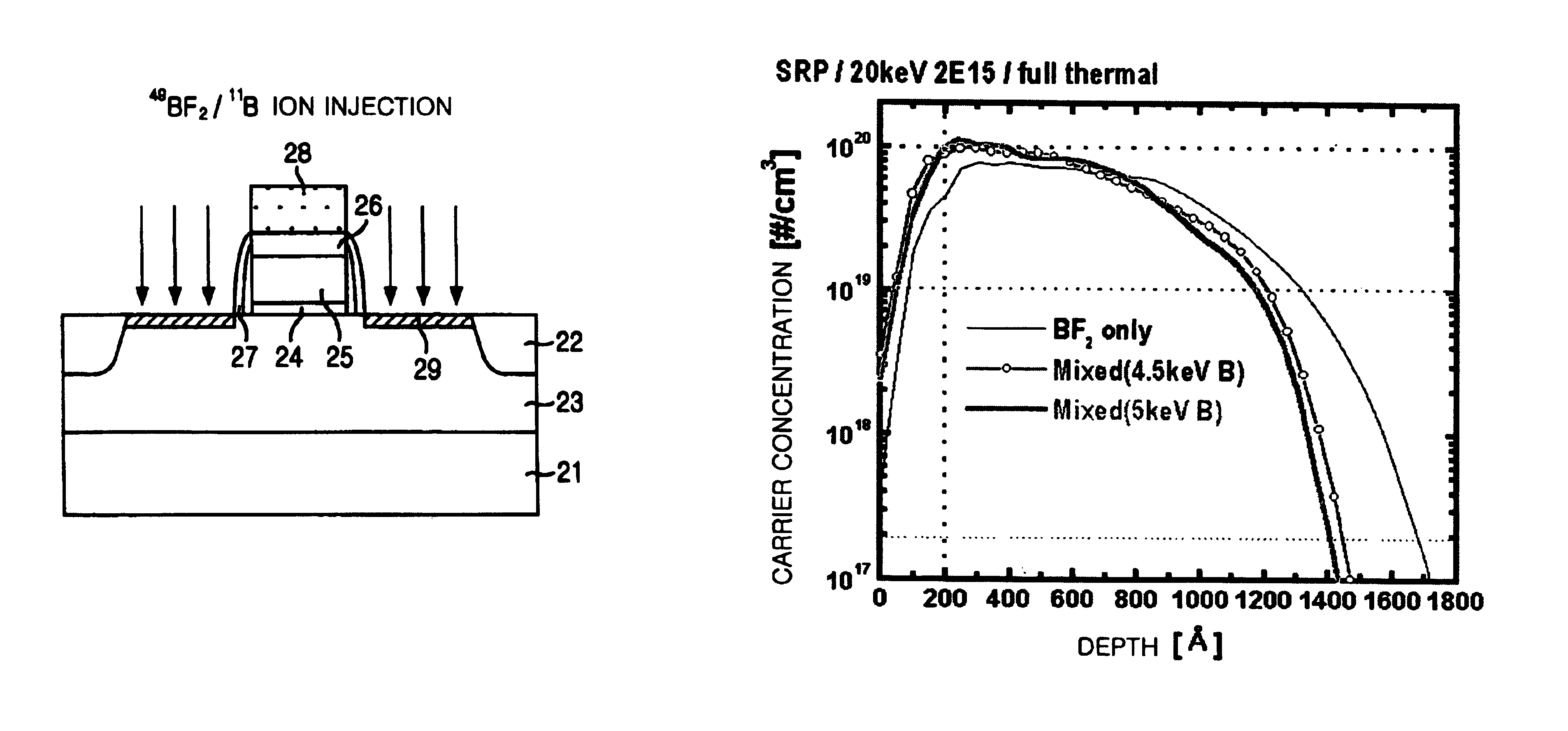
[0031]FIGS. 6A and 6B are cross-sectional views showing a method for manufacturing a transistor of a semiconductor device according to an embodiment of the present invention.

[0032]Referring to FIGS. 6A and 6B, a device isolation layer 22 is formed on a silicon substrate 21 using a trench isolation (STI) process. A p-well (not shown) and an n-well 23 are formed on the silicon substrate 21 through high energy ion implantation. Next, a gate oxide layer 24 and a gate electrode 25 are formed by carrying out a usual gate forming process. At this time, a mask oxide layer 26 is formed on an upper part of the gate electrode 25, and a spacer 27 consisting of an oxide layer and a nitride layer are formed on a sidewall of the gate electrode 25. In the figures, the reference numeral 28 denotes a photore...


PUM


Abstract

The present invention provides a method for manufacturing a semiconductor device capable of acquiring productivity when a p-type source/drain is formed by the implantation of a BF2 and B ions. The method for manufacturing a semiconductor device includes the steps of: implanting a BF2 ion in a p-type source/drain region on a silicon substrate with an ion implantation energy of from about 10 keV to about 20 keV; implanting B ion in the p-type source/drain region with an ion implantation energy of from about 5 keV to about 10 keV; and forming a p-type source/drain by carrying out a thermal treatment.

Description

FIELD OF THE INVENTION[0001]The present invention relates to a semiconductor manufacturing technology; and, more particularly, to a method for forming p+ source / drain region of a metal oxide semiconductor (MOS) transistor.PRIORITY[0002]This application claims the benefit of priority of corresponding Application No. 2001-38758, filed Jun. 30, 2001, Republic of Korea, the contents of which are incorporated herein by reference in their entirety.DESCRIPTION OF THE PRIOR ART[0003]Metal oxide semiconductor (MOS) transistors find widespread use in semiconductor devices, especially in semiconductor memory. The fabrication process of MOS transistors affects their operational characteristics, and the operational characteristics of the devices of which they are a part.[0004]One aspect of MOS transistor fabrication having an influence on MOS transistor performance is the ion implantation process used to form the source / drain regions. Methods for forming source / drain regions using conventional i...

Claims


Application Information

Patent Timeline
Patent Type & Authority Patents(United States)
IPC IPC(8): H01L21/265H01L21/02H01L21/336H01L29/78
CPCH01L21/26513H01L29/6656H01L29/66575H01L21/2658H01L21/265
Inventor OH, JAE-GEUN
Owner SK HYNIX INC
Why Eureka
Try Eureka