Optical multilayer structure, optical switching device, and image display

a multi-layer structure and optical switching technology, applied in static indicating devices, instruments, optical elements, etc., can solve the problems of complex structure, inability to realize light valves in visible light regions, and diffraction grating structure of glv, etc., to achieve simple configuration, small structure, and high response

Inactive Publication Date: 2005-09-06
SONY CORP
View PDF13 Cites 124 Cited by
  • Summary
  • Abstract
  • Description
  • Claims
  • Application Information

AI Technical Summary

Benefits of technology

[0009]The invention has been achieved in consideration of the problems and a first object of the invention is to provide an optical multilayer structure having a simple configuration and

Problems solved by technology

Although a display such as a projector can be realized by using any of the devices, since the operation speed of each a liquid crystal and the DMD is slow, to realize a display as a light valve, the devices have to be arranged two-dimensionally, so that the structure becomes complicated.
However, the GLV has a diffraction grating structure and is therefore complicated, for example, since six devices have to be formed per pixel and diffracted rays emitted in two directions ha

Method used


Image

  • Optical multilayer structure, optical switching device, and image display
  • Optical multilayer structure, optical switching device, and image display
  • Optical multilayer structure, optical switching device, and image display

Examples


first embodiment

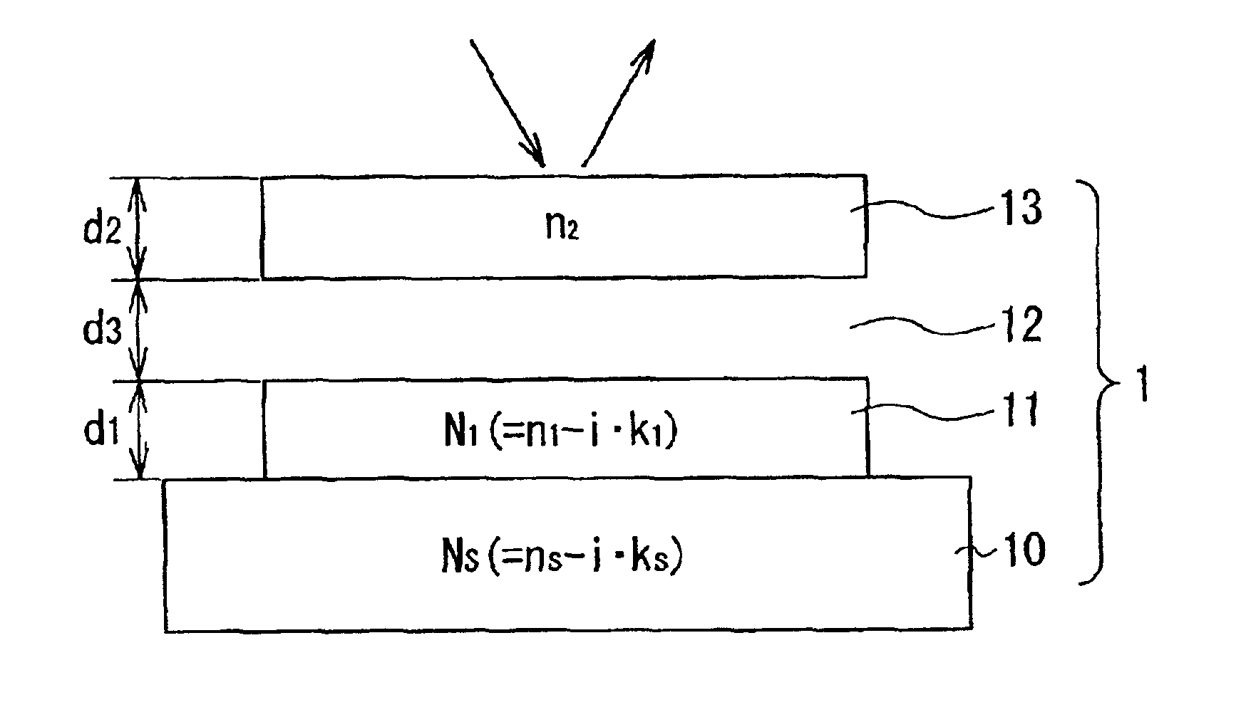
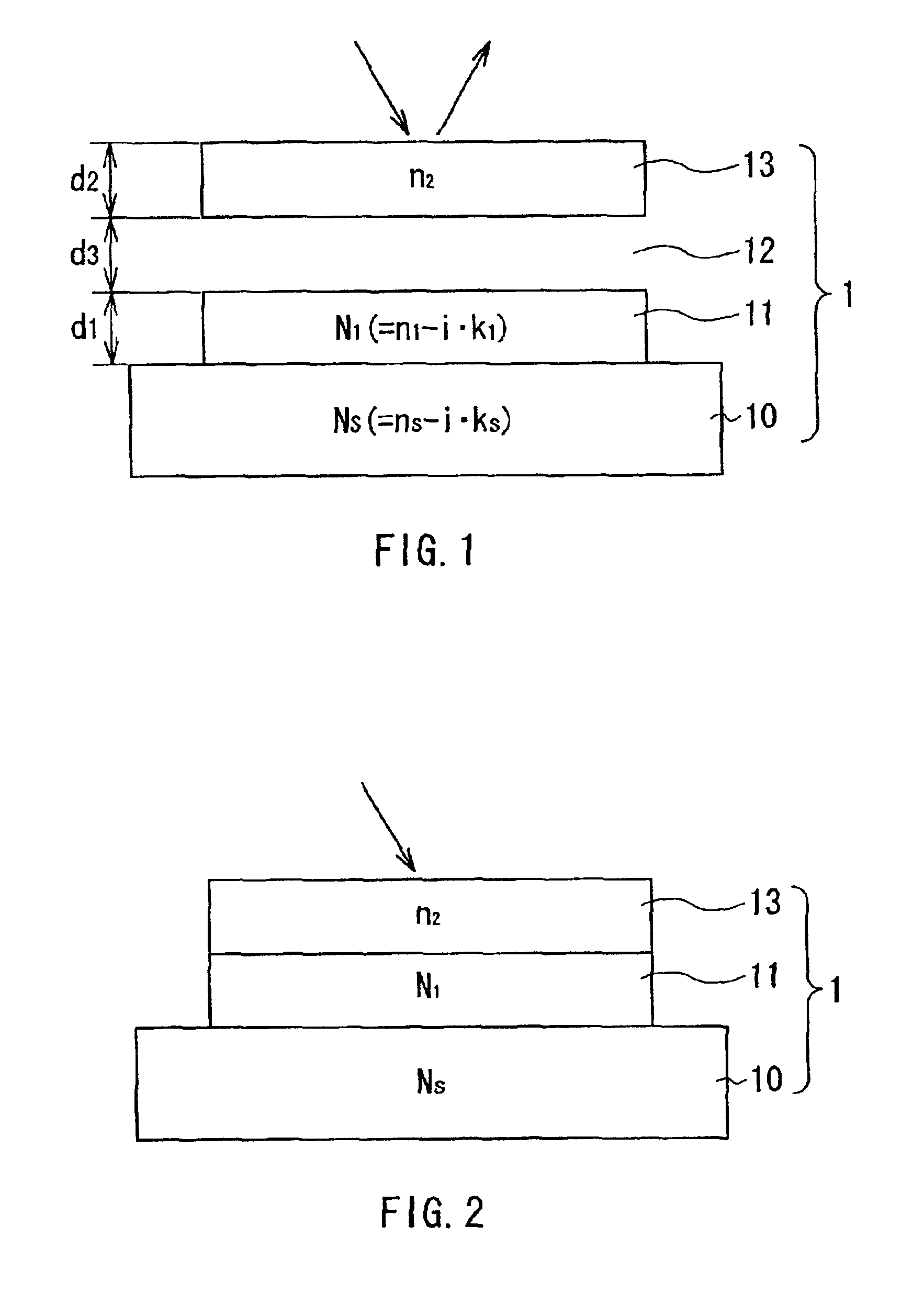
[0098]FIGS. 1 and 2 show a basic configuration of an optical multilayer structure 1 according to a first embodiment of the invention. FIG. 1 shows a high reflectance state where a gap portion 12 described hereinlater in an optical multilayer structure 1 exists. FIG. 2 is a low reflectance state where there is no gap portion 12 of the optical multilayer structure 1. The optical multilayer structure 1 is used as, concretely for example, an optical switching device. By arranging a plurality of optical switching devices one-dimensionally or two-dimensionally, an image display can be constructed. As will be described in detail hereinlater, in the case of fixing the optical multilayer structure 1 in a structure as shown in FIG. 2, it can be used as an antireflection film.

[0099]The optical multilayer structure 1 is constructed by stacking, on a substrate 10, an optical-absorbing first layer 11 in contact with the substrate 10, the gap portion 12 having a changeable size capable of causing ...

concrete examples

[0126]FIG. 8 shows the relation between the wavelength (designed wavelength of 550 nm) of incident light and reflectance in the case of using an opaque carbon substrate (Ns=1.90, k=0.75) as the substrate, a Ta layer (N1=2.46, k=1.90) as the first layer 11, an air layer (n=1.00) as the gap portion 12, and a stacked film (composite refractive index n2=2.0, k=0) of an Si3N4 film and an ITO (Indium-Tin Oxide) film as the second layer 13. (a) indicates a characteristic in the case where an optical film thickness of the gap portion (air layer) is “0” (low reflectance side) and (b) indicates a characteristic in the case where the optical film thickness is “λ / 4” (137.5 nm) (high reflectance side). FIGS. 9 and 10 are optical admittance diagrams shown as a reference. FIG. 9 shows the case of low reflectance. FIG. 10 shows the case of high reflectance.

[0127]As obviously understood from FIG. 8, in the optical multilayer structure 1 of the embodiment, when the optical film thickness of the gap p...

second embodiment

[0164]Each of FIGS. 25 and 26 shows a basic configuration of an optical multilayer structure 2 according to a second embodiment of the invention. FIG. 25 shows a state where a gap portion 53 which will be described hereinlater exists in the optical multilayer structure 2, and FIG. 26 shows a state where there is no gap portion in the optical multilayer structure 2.

[0165]The optical multilayer structure 2 is constructed by stacking, on a substrate 50 made of, for example, a metal, a first transparent layer 51 made of a material having a high refractive index, a second transparent layer 52 made of a material having a low refractive index, a gap portion 53 having a changeable size capable of causing an optical interference phenomenon, and a third transparent layer 54 made of a material having a high refractive index.

[0166]The position of the gap portion 53 is not limited to the example (the position between the second and third transparent layers 52 and 54) but the gap portion 53 may b...


PUM


Abstract

An optical multilayer structure has a substrate, a light-absorbing first layer in contact with the substrate, a gap portion having a changeable size capable of causing an optical interference phenomenon, and a second layer. By changing the size of the gap portion, an amount of reflection, transmission, or absorption of incident light can be changed. For example, the substrate is made of carbon (C), the first layer is made of tantalum (Ta), and the second layer is made of silicon nitride (Si3N4). Also in a visible light area, high response is realized. Consequently, the optical multilayer structure can be suitably used for an image display. The optical multilayer structure may be obtained by stacking, on a substrate made of a metal such as chromium (Cr), a first transparent layer made of a material having a high refractive index such as TiO2 (n=2.40), a second transparent layer made of a material having a low refractive index such as MgF2 (n=1.38), a gap portion having a changeable size capable of causing an optical interference phenomenon, and a third transparent layer made of a material having a high refractive index such as TiO2.

Description

BACKGROUND OF THE INVENTION[0001]1. Field of the Invention[0002]The present invention relates to an optical multilayer structure having a function of reflecting, transmitting, or absorbing incident light, an optical switching device using the same, and an image display using the same.[0003]2. Description of the Related Art[0004]In recent years, importance of a display as a display device of video information is increasing. As a device for the display and, further, as a device for optical communication, an optical memory device, an optical printer, and the like, development of an optical switching device (light valve) operating at high speed is in demand. Conventionally, as devices of this kind, there are a device using a liquid crystal, a device using a micro mirror (digital micro mirror device (DMD), trade mark of Texas Instruments), a device using a diffraction grating (Grating Light Valve (GLV™) of Silicon Light Machines (SLM)), and the like.[0005]A GLV is obtained by fabricating...

Claims


Application Information

Patent Timeline
IPC IPC(8): G02B6/35G02B5/28G02B6/28G02F1/01G02B26/00
CPCG02B5/284G02B5/285G02B5/286G02B6/3512G02B6/3524G02B26/001G02B6/3544G02B6/355G02B6/3572G02B6/3584G02B6/3594
Inventor ISHIKAWA, HIROICHI
Owner SONY CORP
Why Eureka
Try Eureka