Capacitor with enhanced performance and method of manufacture

a capacitor and enhanced technology, applied in the field of semiconductor devices, can solve the problems of high voltage fluctuations in the supply line, noise on the internal signal of the capacitor, and voltage noise on the power supply line, and achieve the effect of improving performan

Inactive Publication Date: 2005-09-06
TAIWAN SEMICON MFG CO LTD
View PDF40 Cites 62 Cited by
  • Summary
  • Abstract
  • Description
  • Claims
  • Application Information

AI Technical Summary

Benefits of technology

[0009]These and other problems are generally solved or circumvented, and technical advantages are generally achieved, by preferred embodiments of the present invention which teach an integrated circuit capacitor with enhanced performance and method of manufacture a capacitor.

Problems solved by technology

During the operation of circuits, the power supply lines must supply transient currents with a relatively high intensity, and can result in voltage noise on the power supply lines.
In such circuits, the rising time of clock signals is very short, so that voltage fluctuations in the supply line can be very large.
Undesired voltage fluctuations in the power supply line powering a circuit can cause noise on its internal signals and degrade noise margins.
The degradation of noise margins can reduce circuit reliability or even cause circuit malfunction.
Integrated chips fabricated on bulk substrates can naturally decouple the power supply potential and the ground potential due to the presence of inherent depletion capacitances between the doped wells and the bulk substrate.

Method used


Image

  • Capacitor with enhanced performance and method of manufacture
  • Capacitor with enhanced performance and method of manufacture
  • Capacitor with enhanced performance and method of manufacture

Examples


Embodiment Construction

[0025]The making and using of the presently preferred embodiments are discussed in detail below. It should be appreciated, however, that the present invention provides many applicable inventive concepts that can be embodied in a wide variety of specific contexts. The specific embodiments discussed are merely illustrative of specific ways to make and use the invention, and do not limit the scope of the invention.

[0026]In the preferred embodiment this invention, a capacitor structure with at least one strained electrode is taught. The strained electrode may, for example, be comprised of a strained silicon layer. For example, the strained electrode can be a heavily doped strained silicon layer or it can be an inversion layer in a strained silicon layer.

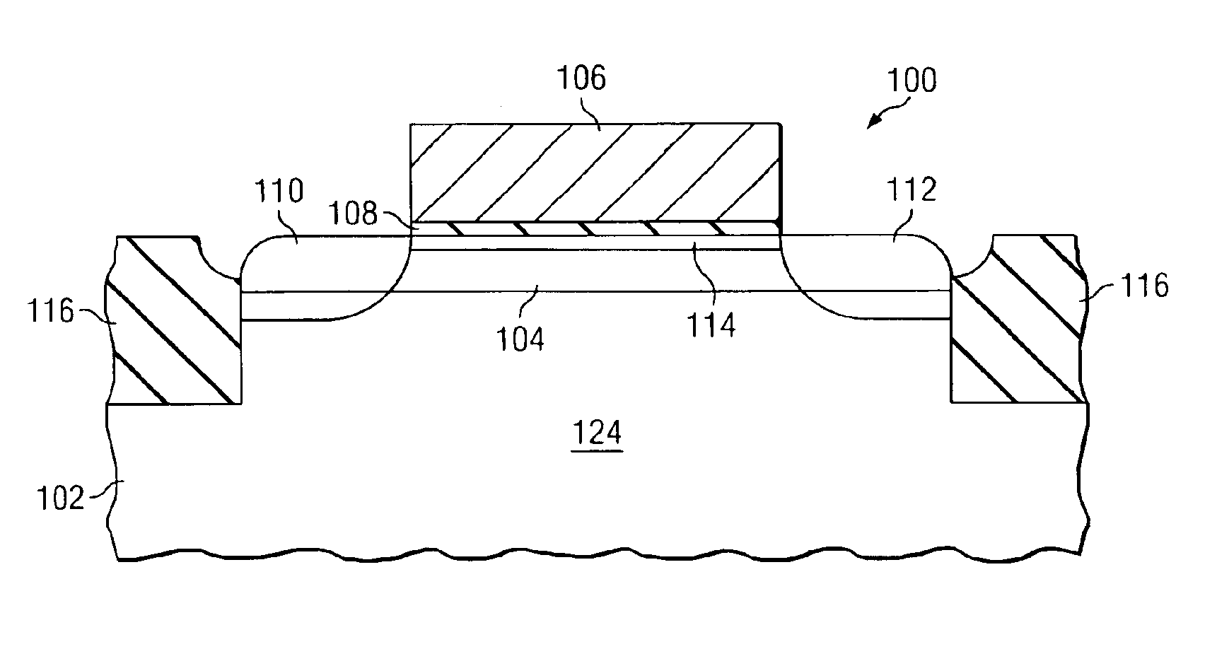
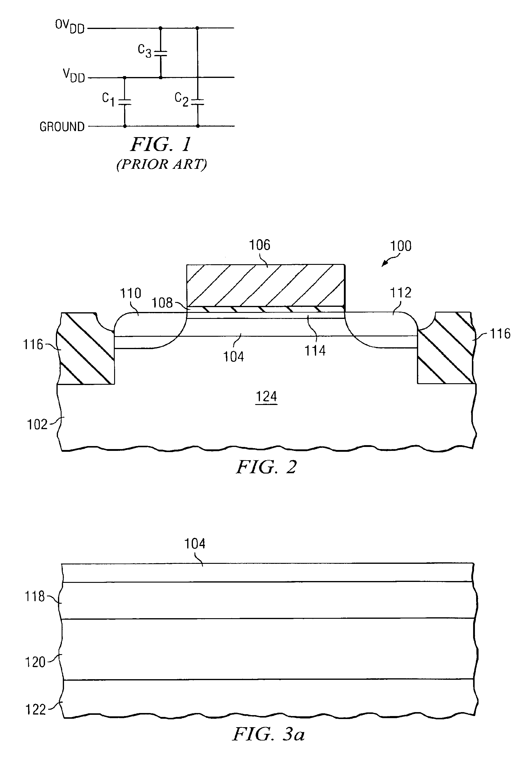
[0027]FIG. 2 shows a specific embodiment of this invention. FIG. 2 shows a semiconductor substrate 102 with a top strained silicon layer 104. A capacitor 100 is formed on substrate 102 and includes top electrode 106 that overlies a capac...


PUM

PropertyMeasurementUnit
thicknessaaaaaaaaaa
thicknessaaaaaaaaaa
relative permittivityaaaaaaaaaa

Abstract

A decoupling capacitor is formed in a semiconductor substrate that includes a strained silicon layer. A substantially flat bottom electrode is formed in a portion of the strained silicon layer and a capacitor dielectric overlying the bottom electrode. A substantially flat top electrode overlies said capacitor dielectric. The top electrode is connected to a first reference voltage line and the bottom electrode is connected to a second reference voltage line.

Description

CROSS-REFERENCE TO RELATED APPLICATIONS[0001]This application relates to co-pending and commonly assigned patent application Ser. No. 10 / 628,020, filed Jul. 23, 2003, and entitled “Capacitor with Improved Capacitance Density and Method of Manufacture” , which application is hereby incorporated herein by reference.TECHNICAL FIELD[0002]The present invention relates generally to semiconductor devices and more particularly to a capacitor with enhanced performance and method of manufacture.BACKGROUND[0003]Power supply lines in a semiconductor integrated circuit chip supply current to charge and discharge active and passive devices in the integrated circuit. For example, digital complementary metal-oxide-semiconductor (CMOS) circuits draw current when the clock makes a transition. During the operation of circuits, the power supply lines must supply transient currents with a relatively high intensity, and can result in voltage noise on the power supply lines. The voltage on the power suppl...

Claims


Application Information

Patent Timeline
Patent Type & Authority Patents(United States)
IPC IPC(8): H01L29/66H01L21/02H01L27/08H01L29/94
CPCH01L27/0805H01L28/40H01L29/94Y10T29/435H01L2924/0002H01L2924/00
Inventor YEO, YEE-CHIAHU, CHENMING
Owner TAIWAN SEMICON MFG CO LTD
Why Eureka
Try Eureka