Check patentability & draft patents in minutes with Patsnap Eureka AI!

Pattern forming method

a pattern and forming technology, applied in the field of pattern forming methods, can solve problems such as the decrease of pattern forming accuracy, and achieve the effect of high throughput and high accuracy

Inactive Publication Date: 2005-09-06
KK TOSHIBA
View PDF20 Cites 7 Cited by
  • Summary
  • Abstract
  • Description
  • Claims
  • Application Information

AI Technical Summary

Benefits of technology

[0011]The present invention has an object of providing a pattern forming method capable of forming a fine small pattern with high accuracy at a high throughput.
[0012]In order to achieve both down-sizing and improvement of a throughput, light exposure and charge beam exposure are sometimes used together. In this case, a difference in exposure position between the light exposure and the charge exposure leads to a decrease of pattern forming accuracy. According to the present invention, when exposure of a second pattern is performed after exposure of a first pattern, the exposure position of the second pattern is adjusted on the basis of a latent image of the first pattern which has already been subjected to exposure. As a result, a positional displacement between the first and second pattern can be reduced so that a desired pattern can be formed with high accuracy.
[0013]In addition, a displacement of an exposure position of a pattern can be reduced by directly adjusting the exposure position of a pattern, based on a surface pattern on a substrate.
[0015]Instead of the manner as described above, it is possible to prevent formation of an unnecessary exposed portion itself, by detecting a latent image or a surface pattern with use of light having a wavelength which cannot be sensed by a sensitive material, or by setting an irradiation amount of light to a value smaller than an irradiation amount with which a sensitive material is exposed.
[0016]Further, if the position of a latent image thus obtained is displaced by a predetermined distance or more from a designed position, the sensitive material is peeled, and coating of a sensitive material and exposure thereof are performed again. In this manner, wasteful development processing can be prevented and omitted, and the throughput can be improved thereby.

Problems solved by technology

In this case, a difference in exposure position between the light exposure and the charge exposure leads to a decrease of pattern forming accuracy.

Method used


Image

  • Pattern forming method
  • Pattern forming method
  • Pattern forming method

Examples


Embodiment Construction

[0054]In the following, preferred embodiments of the present invention will be explained with reference to the drawings. At first, a Mix and Match method as a base of the present invention depending on light exposure and electron beam (EB) exposure will be briefly explained.

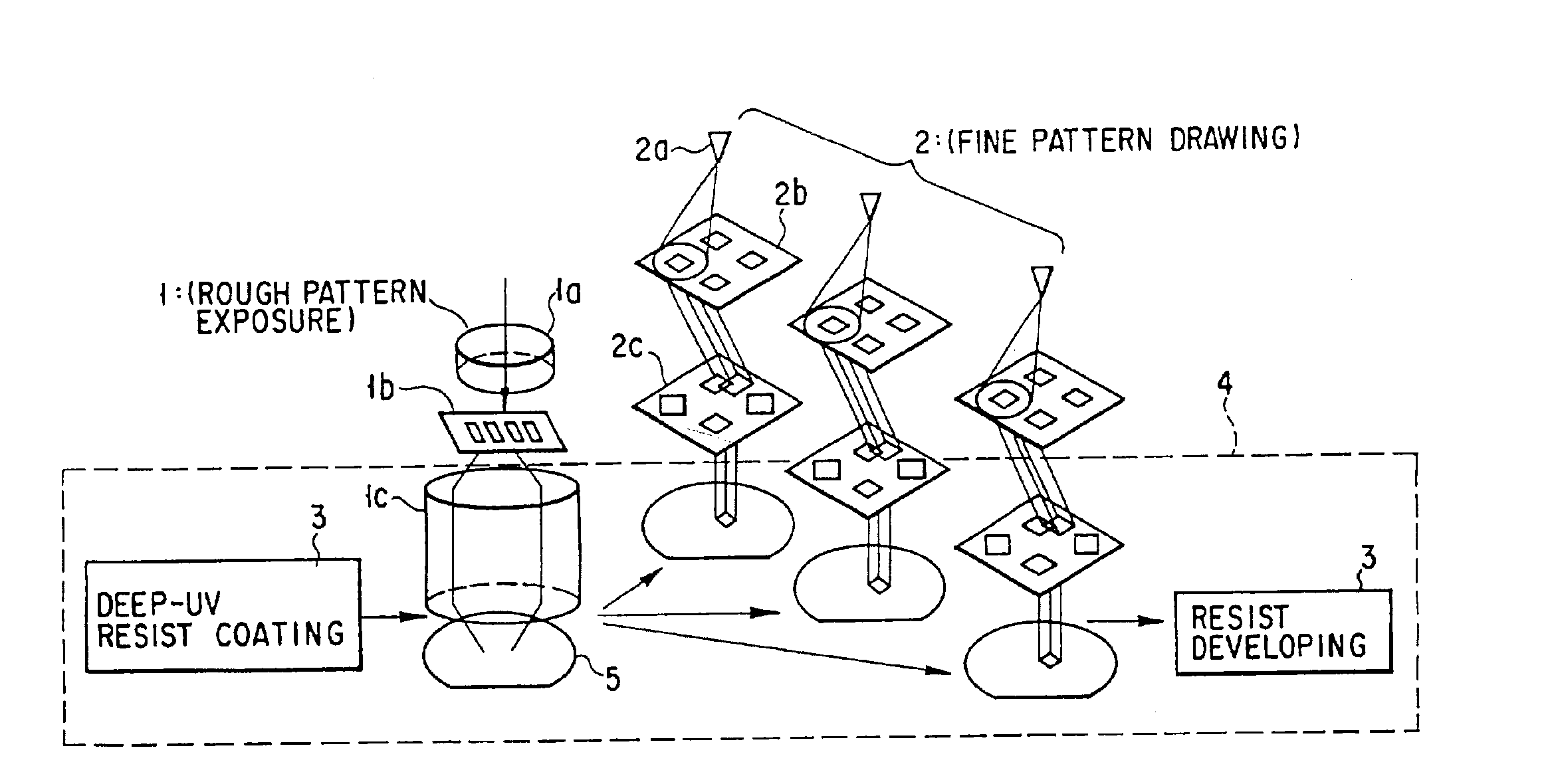
[0055]FIGS. 1 and 2 are views explaining the Mix and Match method. In the figures, a reference 1 denotes a light stepper consisting of, for example, a deep-UV stepper. A reference 2 denotes an electron beam exposure device adopting a cell-projection method, and a plurality of devices 2 are provided. A reference 3 denotes a resist coating / developing device for coating a resist and a anti-reflection film and for developing a resist coated with a pattern. A reference 4 is a transport mechanism for transporting wafers between devices 1, 2, and 3 in an environment under atmospheric control, in order to process a resist by in-line processing. A reference 5 denotes a semiconductor wafer as a substrate to be processed.

[0...


PUM

PropertyMeasurementUnit
thicknessaaaaaaaaaa
energyaaaaaaaaaa
acceleration voltageaaaaaaaaaa

Abstract

To achieve down-sizing and improvements of throughputs, light exposure and charge beam exposure are sometimes used together. In case of performing exposure of a desired pattern in a plurality of stages, a positional displacement of each of exposure patterns in the stages leads to a decrease in exposure accuracy. According to the present invention, in case of forming a fine pattern by exposure after exposure of a rough pattern, the exposure position of the rough pattern is adjusted, based on a latent image of the rough pattern which has been subjected to exposure. As a result, a positional-displacement between rough and fine patterns is reduced so that a desired pattern can be formed with high accuracy.

Description

CROSS REFERENCE TO RELATED APPLICATION[0001]This application is a CON of Ser. No. 09 / 670,098, Sep. 26, 2000 and now ABN, which is a DIV of Ser. No. 09 / 379,098, Aug. 23, 1999, U.S. Pat. No. 6,147,355, which is a DIV of Ser. No. 09 / 030,886, Feb. 26, 1998, U.S. Pat. No. 5,989,759.BACKGROUND OF THE INVENTION[0002]The present invention relates to a pattern forming method for forming patterns of a semiconductor integrated circuit, including a fine small pattern, with a high accuracy and a high throughput.[0003]In a semiconductor manufacture method, an optical lithography has been used widely for manufacturing devices because of its processing simplicity and low cost. Technical developments have been continuously made, and in recent years, downsizing of an element to 0.25 μm or less has come to be nearly achieved by introducing short waves (e.g., by a KrF excimer laser light source). To further prosecuting the downsizing, developments in ArF excimer laser light sources using a much shorter...

Claims


Application Information

Patent Timeline
Patent Type & Authority Patents(United States)
IPC IPC(8): G03F7/20H01J37/30H01J37/304H01J37/317H01L21/027
CPCH01J37/3174B82Y10/00B82Y40/00G03F7/7045G03F7/70675H01J37/3045Y10S430/143
Inventor ANDO, ATSUSHISUGIHARA, KAZUYOSHIOKUMURA, KATSUYANAKASUGI, TETSURO
Owner KK TOSHIBA
Features
  • R&D
  • Intellectual Property
  • Life Sciences
  • Materials
  • Tech Scout
  • Unparalleled Data Quality
  • Higher Quality Content
  • 60% Fewer Hallucinations
Learn More