Semiconductor device and method for fabricating the same

Active Publication Date: 2005-09-13
TAIWAN SEMICON MFG CO LTD
View PDF11 Cites 22 Cited by
  • Summary
  • Abstract
  • Description
  • Claims
  • Application Information

AI Technical Summary

Benefits of technology

[0024]In view of the above-described problems, it is therefore an object of the present invention that in a semiconductor device that includes a capacitive insulating film using ferroelectric or high dielectric material, deterioration, d

Problems solved by technology

However, ferroelectric materials and high dielectric materials, which are oxides whose crystal structure determines the physical characteristics thereof, are affected greatly by hydrogen reduction.
However, as in the first and second prior art examples, in a structure in which a hydrogen-barrier layer is provided to the lateral portion of the capacitors as well, to cover each capacitor element itself, or with plurali

Method used


Image

  • Semiconductor device and method for fabricating the same
  • Semiconductor device and method for fabricating the same
  • Semiconductor device and method for fabricating the same

Examples


Example

[0121](First Embodiment)

[0122]Hereinafter, a first embodiment of the present invention will be described with reference to the accompanying drawings.

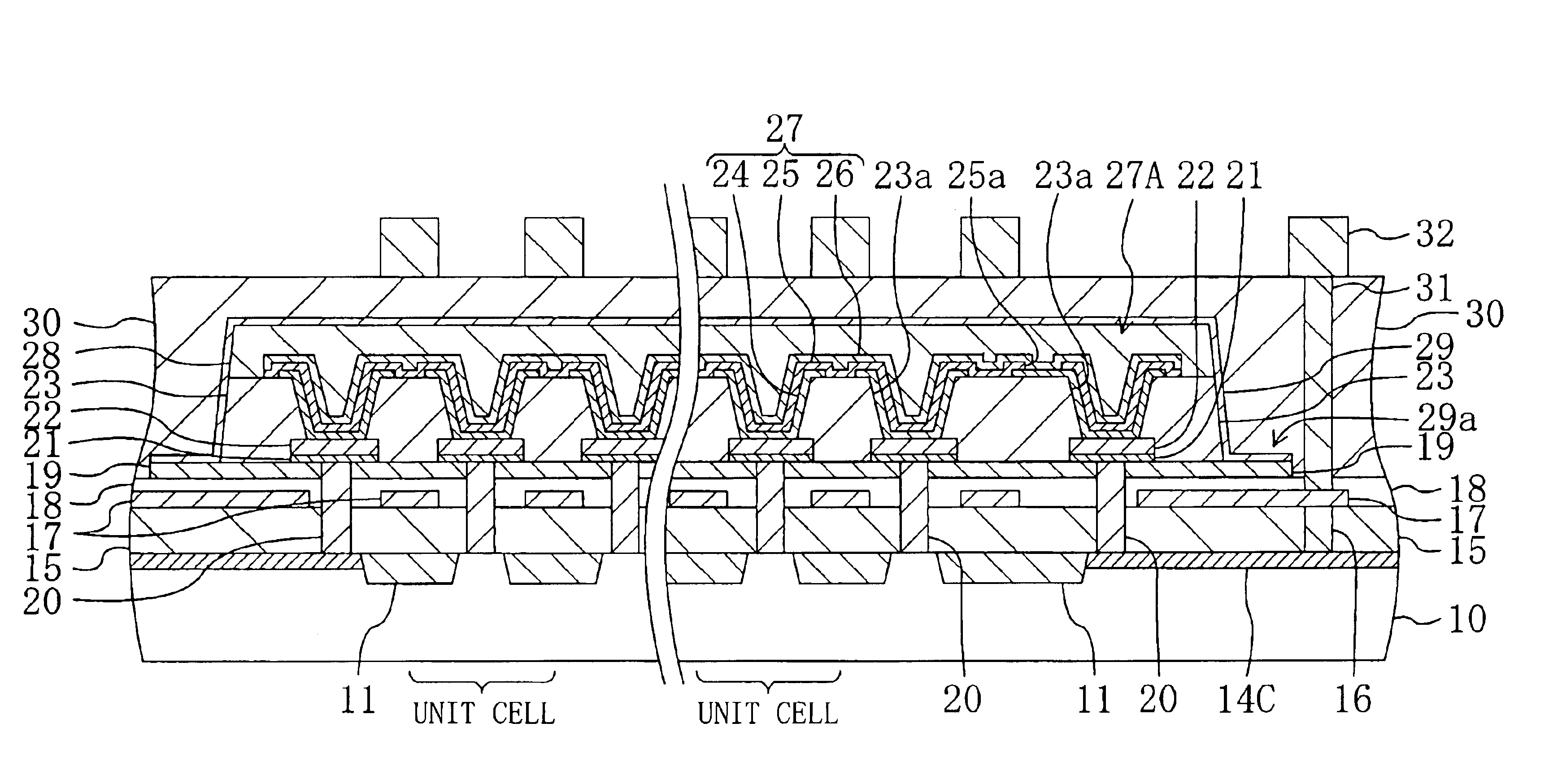
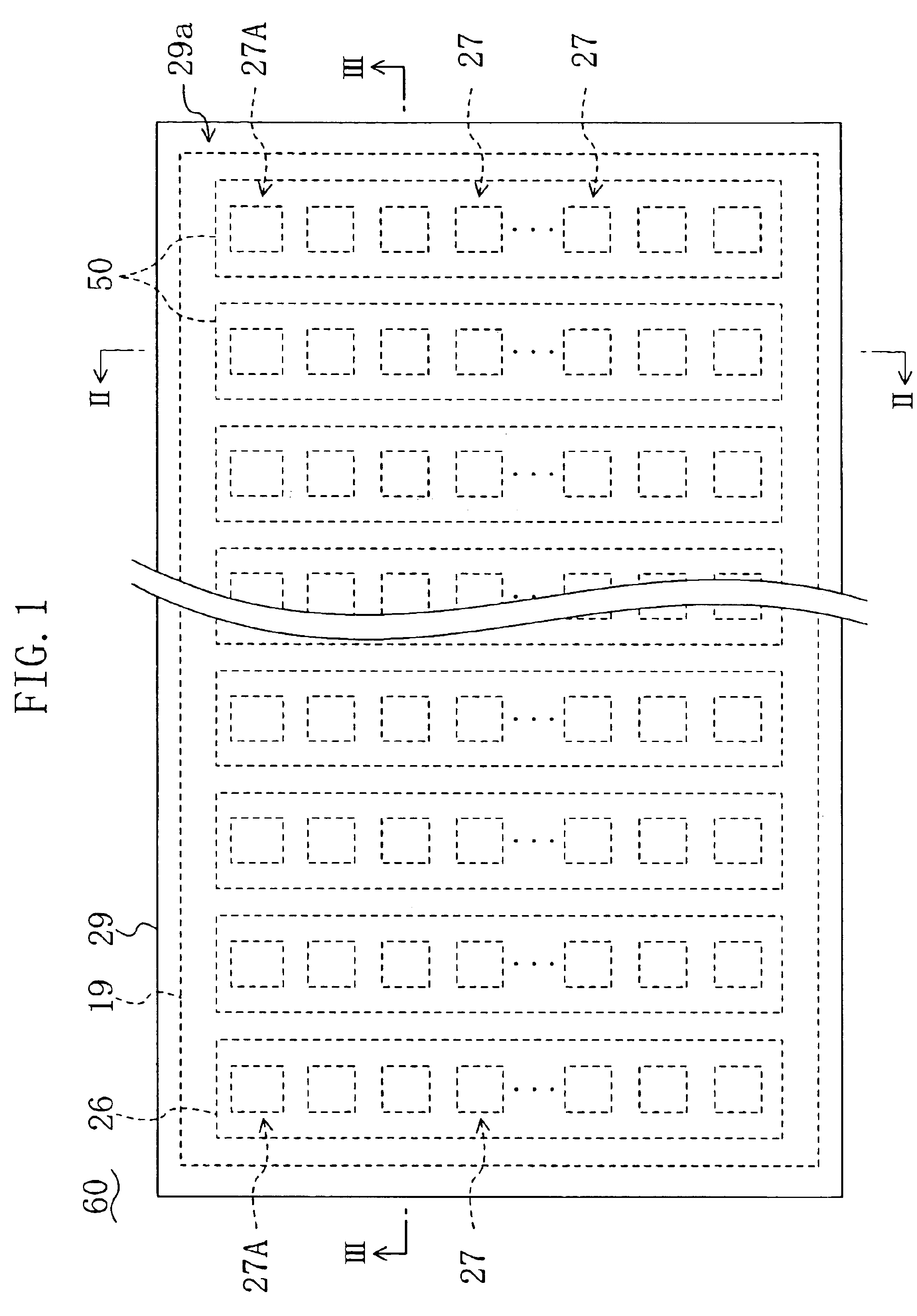
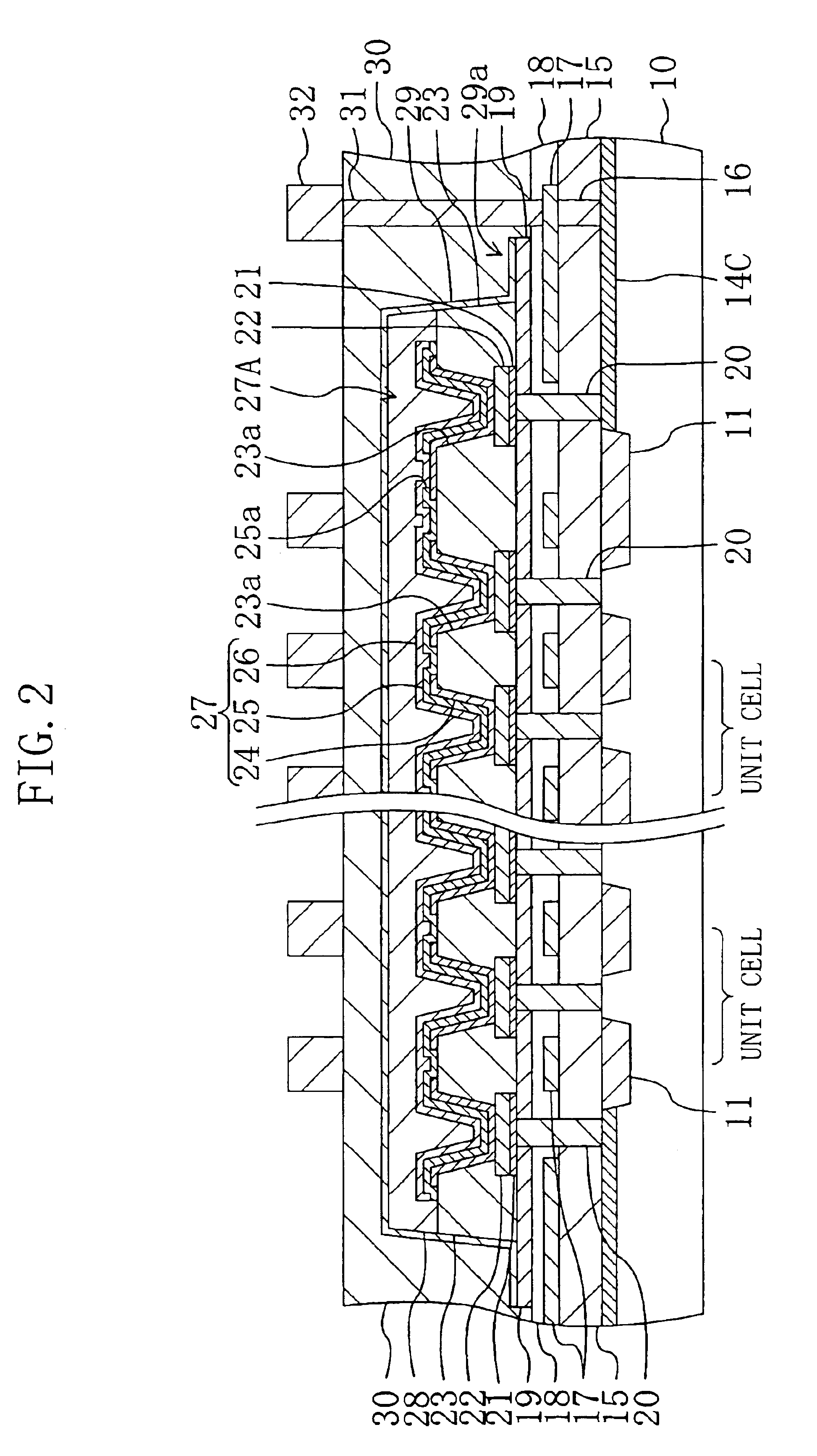
[0123]FIG. 1 illustrates the plan configuration of a cell block in a semiconductor device in accordance with the first embodiment of the present invention. FIG. 2 illustrates the cross-sectional structure taken along the line II—II of FIG. 1, while FIG. 3 illustrates the cross-sectional structure taken along the line III—III of FIG. 1.

[0124]As shown in FIG. 1, an insulative lower hydrogen-barrier film 19 of silicon nitride (Si3N4) is formed over a semiconductor substrate of silicon (Si), for example. Over the insulative lower hydrogen-barrier film 19, a plurality of capacitors 27 are provided in the form of a matrix.

[0125]In each of the capacitor 27 groups that are disposed in the direction intersecting the direction in which bit lines extend, as will be described later, sixty-five upper electrodes, for example, are connected with each ...

Example

[0196](Second Embodiment)

[0197]Hereinafter, a second embodiment of the present invention will be described with reference to the accompanying drawings.

[0198]FIG. 11 shows a partial cross-sectional structure of a semiconductor device in accordance with the second embodiment of the present invention. In FIG. 11, the same members as those shown in FIG. 3 are identified by the same reference numerals and the description thereof will be omitted herein.

[0199]In the semiconductor device of the second embodiment, conductive lower hydrogen-barrier films 21, which cover the upper surfaces of second contact plugs 20 that are connected to doped source regions 14B of MOS transistors or doped interconnect layers 14C, are formed directly on a second interlayer dielectric film 18 that covers bit lines 17. Further, an insulative lower hydrogen-barrier film 39 of titanium aluminum oxide is formed on the second interlayer dielectric film 18 so that the insulative lower hydrogen-barrier film 39 covers ...

Example

[0209](Third Embodiment)

[0210]Hereinafter, a third embodiment of the present invention will be described with reference to the accompanying drawings.

[0211]FIG. 14 illustrates a partial cross-sectional structure of a semiconductor device in accordance with the third embodiment of the present invention. In FIG. 14, the same members as those shown in FIG. 3 are identified by the same reference numerals and the description thereof will be omitted herein.

[0212]The semiconductor device of the third embodiment employs a structure in which conductive lower hydrogen-barrier films 40a, each made of an about 50 nm thick film of titanium aluminum nitride, are provided in the lateral and lower portions of second contact plugs 40 that are connected to doped source regions 14B of MOS transistors and doped interconnect layers 14C. In each of the second contact plugs 40, a contact plug body 40b of tungsten is formed.

[0213]Further, an oxygen-barrier film 42, composed of, from the bottom layer, an abo...


PUM


Abstract

A semiconductor device includes: a lower hydrogen-barrier film; a capacitor formed on the lower hydrogen-barrier film and including a lower electrode, a capacitive insulating film, and an upper electrode; an interlayer dielectric film formed so as to cover the periphery of the capacitor; and an upper hydrogen-barrier film covering the top and lateral portions of the capacitor. An opening, which exposes the lower hydrogen-barrier film where the lower hydrogen-barrier film is located around the capacitor, and which is tapered and flares upward, is formed in the interlayer dielectric film, and the upper hydrogen-barrier film is formed along the lateral and bottom faces of the opening, and is in contact with the lower hydrogen-barrier film in the opening.

Description

BACKGROUND OF THE INVENTION[0001]The present invention relates to semiconductor devices in which a ferroelectric material or a high dielectric material is used for a capacitive insulating film, and methods for fabricating the devices.[0002]Semiconductor devices in which a ferroelectric material or a high dielectric material is used for a capacitive insulating film have residual polarization that exhibits hysteresis characteristics, and a high dielectric constant. Such semiconductor devices therefore may replace semiconductor devices that have a capacitive insulating film made of silicon oxide or silicon nitride, in the field of nonvolatile memory devices and DRAM devices.[0003]However, ferroelectric materials and high dielectric materials, which are oxides whose crystal structure determines the physical characteristics thereof, are affected greatly by hydrogen reduction. Nevertheless, MOS-transistor formation process, multilevel-interconnect formation process, and passivation-film f...

Claims


Application Information

Patent Timeline
IPC IPC(8): H01L21/70H01L27/115H01L21/8246H01L21/02H01L21/8242
CPCH01L27/105H01L27/10852H01L27/11502H01L28/65H01L27/11509H01L28/55H01L28/57H01L27/11507H01L27/10894H10B12/033H10B12/09H10B53/40H10B53/30H10B53/00
Inventor ITO, TOYOJIFUJII, EIJIUMEDA, KAZUO
Owner TAIWAN SEMICON MFG CO LTD
Why Eureka
Try Eureka