
Method of peeling off and method of manufacturing semiconductor device

a technology of peeling off and manufacturing method, which is applied in the direction of semiconductor devices, electrical devices, transistors, etc., can solve the problems of difficult and heavy cracking, inability to form any tft with electric characteristics, and difficulty in cracking and heavyness

Inactive Publication Date: 2005-09-20
SEMICON ENERGY LAB CO LTD
View PDF25 Cites 190 Cited by
  • Summary
  • Abstract
  • Description
  • Claims
  • Application Information

AI Technical Summary

Benefits of technology

[0010]The invention has been completed in consideration of the above-described problems and the invention aims to provide a peeling method without damaging a peeled off layer and to allow separation of not only a peeled off layer having a small surface area but also the entire surface of a peeled off layer having a large surface area.

Problems solved by technology

Today, although a glass substrate, a quartz substrate and the like are used in many cases, they have disadvantages that they are easy to crack and heavy.
Further, in terms of mass production, the glass substrate, the quartz substrate and the like are difficult and unsuitable for enlargement.
However, since the heat resistance of the plastic film is low, the highest temperature for process is required to be low and consequently, it is presently impossible to form any TFT with electric characteristics as excellent as those formed on a glass substrate.
In order to transmit energy through the substrate and supply energy sufficient to release hydrogen contained in the amorphous silicon, relatively intense laser beam has to be radiated, resulting in a problem that the peeled off layer is damaged.
As a result, there is a possibility of insufficient peeling-off, even if laser beam is radiated to the isolation layer.
Subsequently, attributed to retention of the quantity of hydrogen contained in the isolation layer, there occurs a problem that the process after isolation layer formation may be limited.
In such a case, it becomes difficult to fabricate a transmission type liquid crystal display apparatus.
Additionally, by the above-described method, peeling of the peeled off layer having a large surface area becomes difficult.

Method used


Image

  • Method of peeling off and method of manufacturing semiconductor device
  • Method of peeling off and method of manufacturing semiconductor device
  • Method of peeling off and method of manufacturing semiconductor device

Examples


embodiment 1

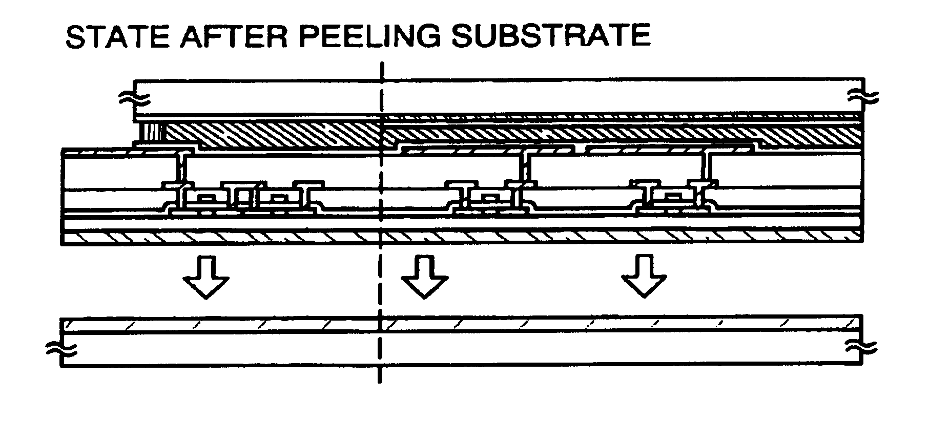
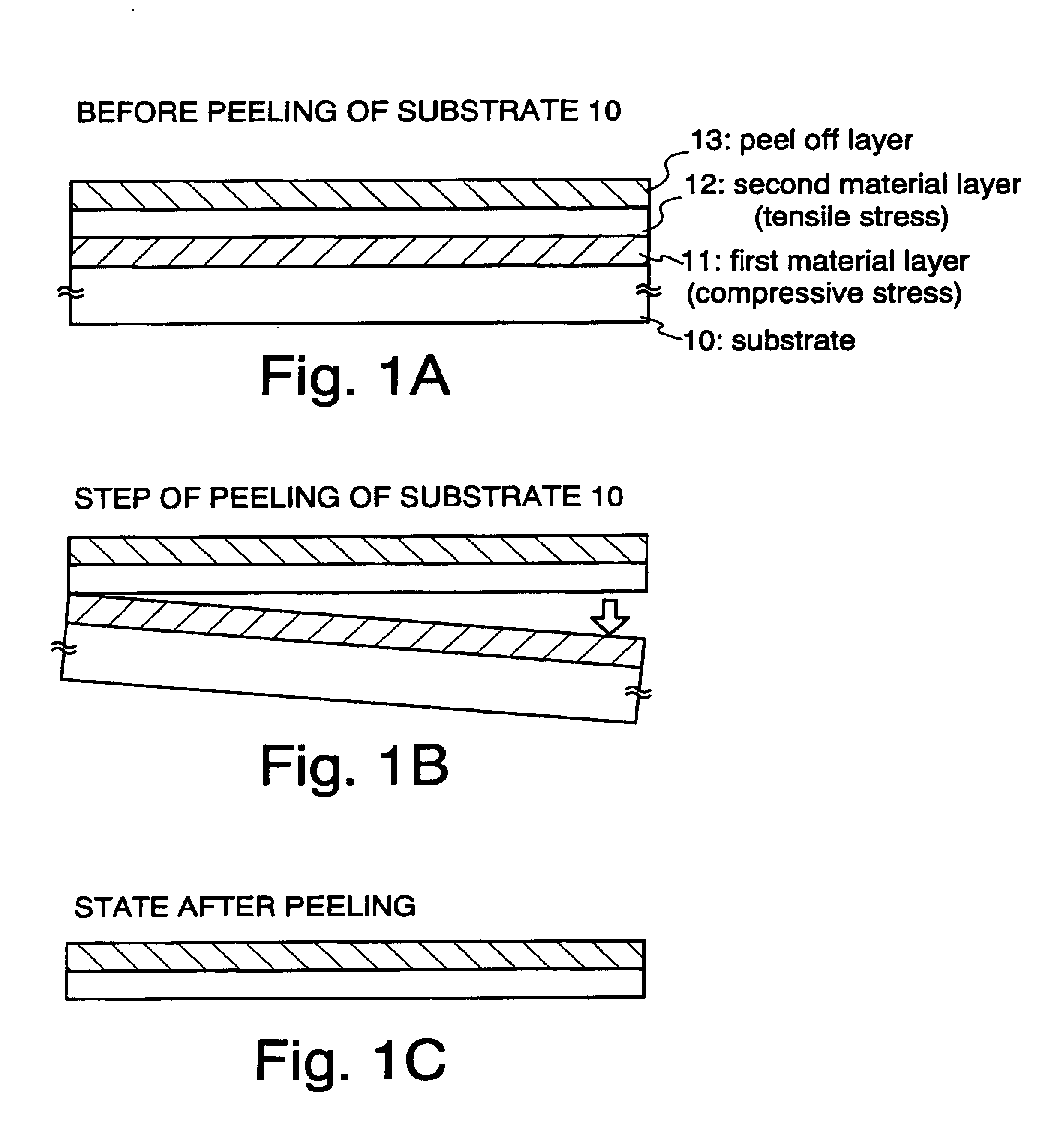
[0084]Hereinafter, typical peeling procedures of the invention will be described concisely with reference to FIG. 1

[0085]In FIG. 1A, the reference numeral 10 denotes a substrate, 11 denotes a first material layer having a tensile stress, 12 denotes a material layer having a compressive stress, and 13 denotes a peeled off layer.

[0086]In FIG. 1A, the substrate 10 may be a quartz substrate, a ceramic substrate or the like. Further, a silicon substrate, a metal substrate, or a stainless steel substrate may be used.

[0087]At first, as illustrated in FIG. 1A, the first material layer 11 is formed on the substrate 10. The first material layer 11 may have a tensile stress even if it has a compressive stress immediately after film formation and it is important for the layer to use a material causing no abnormality such as peeling by heating treatment or laser beam radiating treatment in the peeled off layer formation and having a tensile stress in a range of 1 to 1×10¹⁰ (Dyne / cm2) after the p...

embodiment 2

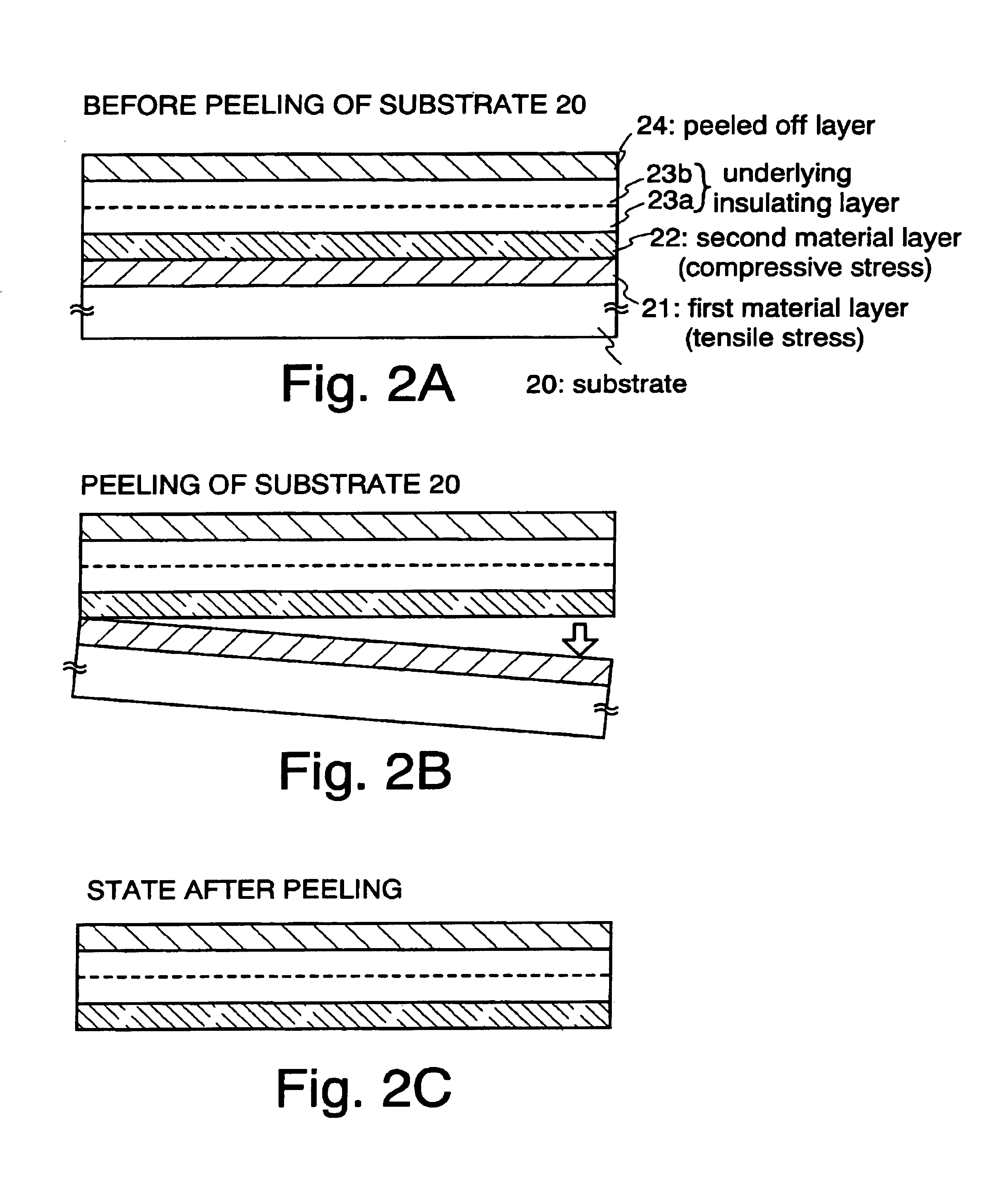
[0098]In this embodiment, the peeling procedure for peeling a substrate while preventing diffusion of impurities from a first material layer and the substrate after an underlying insulating layer is formed adjacently to a peeled off layer will concisely be described with reference to FIG. 2.

[0099]In FIG. 2A, the reference numeral 20 denotes a substrate, 21 denotes a first material layer having a tensile stress, 22 denotes a second material layer having a compressive stress, 23a and 23b each denote an underlying insulating layer, and 24 denotes a peeled off layer.

[0100]In FIG. 2A, the substrate 20 may be a glass substrate, a quartz substrate, a ceramic substrate or the like. Further, a silicon substrate, a metal substrate, or a stainless steel substrate may be used.

[0101]At first, as illustrated in FIG. 2A, the first material layer 21 is formed on the substrate 20. The first material layer 21 may have a compressive stress or a tensile stress immediately after film formation and it is...

embodiment 3

[0115]In this embodiment, in addition to the embodiment 1, an example where laser beam radiating or heating treatment is carried out in order to promote peeling will be described with reference to FIG. 4.

[0116]In FIG. 4A, the reference numeral 40 denotes a substrate, 41 denotes a first material layer, 42 denotes a second material layer, and 43 denotes a peeled off layer.

[0117]Since the process to form up to the peeled off layer 43 is same as that in the embodiment 1, the description will be omitted.

[0118]After the peeled off layer 43 is formed, laser beam radiation is carried out (FIG. 3A). Laser beam to be employed includes gas laser such as excimer laser, solid laser of YVO4 laser, YAG laser, and semiconductor laser. The state of laser oscillation may be both continuous oscillation and pulsed oscillation and the shape of the laser beam is also optionally linear, rectangular, circular, or elliptical. The wavelength to be employed may be fundamental, second higher harmonics, or thir...


PUM


Abstract

The invention aims to provide a peeling method without damaging a peeled off layer and to allow separation of not only a peeled off layer having a small surface area but also the entire surface of a peeled off layer having a large surface area. Further, the invention aims to provide a lightweight semiconductor device by sticking a peeled off layer to a variety of substrates and its manufacturing method. Especially, the invention aims to provide a lightweight semiconductor device by sticking a variety of elements such as TFT to a flexible film and its manufacturing method. Even in the case a first material layer 11 is formed on a substrate and a second material layer 12 is formed adjacently to the foregoing first material layer 11, and further, layered film formation, heating treatment at 500° C. or higher or laser beam radiating treatment is carried out, if the first material layer has a tensile stress before the peeling and the second material layer has a compressive stress, excellent separation can easily be carried out by physical means in the interlayer or interface of the second material layer 12.

Description

BACKGROUND OF THE INVENTION[0001]1. Field of the Invention[0002]The present invention relates to a peeling method of a peeled off layer, especially, a peeling method of a peeled off layer containing various elements. In addition to that, the present invention relates to a semiconductor device comprising a circuit composed of a thin film transistor (hereinafter referred to as TFT) transferred by sticking a separated peeled off layer to a substrate and its manufacturing method. The invention relates, for example, an electrooptical device such as a liquid crystal module, a light emitting device such as an EL module, and an electronic appliance containing such devices as components therein.[0003]The term semiconductor device, in this specification, covers any device as a whole capable of functioning by utilizing semiconductor characteristics and an electrooptical device, a light emitting device, a semiconductor circuit, and electronic apparatus are all included in the semiconductor devi...

Claims


Application Information

Patent Timeline
IPC IPC(8): H01L21/70H01L21/762H01L27/12H01L21/84H01L29/786H01L21/77
CPCH01L21/76251H01L27/1214H01L27/1266H01L29/786
Inventor TAKAYAMA, TORUMARUYAMA, JUNYAYAMAZAKI, SHUNPEI
Owner SEMICON ENERGY LAB CO LTD
Features
  • Generate Ideas
  • Intellectual Property
  • Life Sciences
  • Materials
  • Tech Scout
  • Unparalleled Data Quality
  • Higher Quality Content
  • 60% Fewer Hallucinations
Learn More