System level in-situ integrated dielectric etch process particularly useful for copper dual damascene

a dielectric etching and integrated technology, applied in the field ofplasma etching processes, can solve the problems of significant cost of ownership benefits, undesirable isotropic etching effect on the dielectric layer, and overetching of the dielectric layer including the loss of critical dimensions, so as to reduce the cost of ownership and improve the etching

Inactive Publication Date: 2005-09-27
APPLIED MATERIALS INC
View PDF27 Cites 67 Cited by
  • Summary
  • Abstract
  • Description
  • Claims
  • Application Information

AI Technical Summary

Benefits of technology

[0019]The inventors have found that such a two chamber in situ approach has a reduced cost of ownership as compared to either previously known ex situ systems or single chamber in situ systems. The inventors have also found that such a two chamber in situ approach provides improved etch results as

Problems solved by technology

This analysis concluded that a system-level in situ approach that used two separate chambers in a multichamber system that transferred substrates between chambers under vacuum conditions presented significant cost of ownership benefits over either a multiple chamber ex situ approach or a single, all-in-one chamber approach.
When an all-in-one chamber approach is used, the inventors have found that during the subsequent oxygen stripping process, oxygen may react with and release fluorine from this polymer, which in turn, has an undesirable isotropic etching effect on the dielectric layer.
This isotropic etching effect may result in an overetching of the dielectric layer including the loss of critical dimensions.
Such a technique increases the cost of ownership COO of the tool, however, as the time required to perform such a clean step reduces throughput of the tool.
The addition of oxygen to the etchant

Method used


Image

  • System level in-situ integrated dielectric etch process particularly useful for copper dual damascene
  • System level in-situ integrated dielectric etch process particularly useful for copper dual damascene
  • System level in-situ integrated dielectric etch process particularly useful for copper dual damascene

Examples


invention example 1

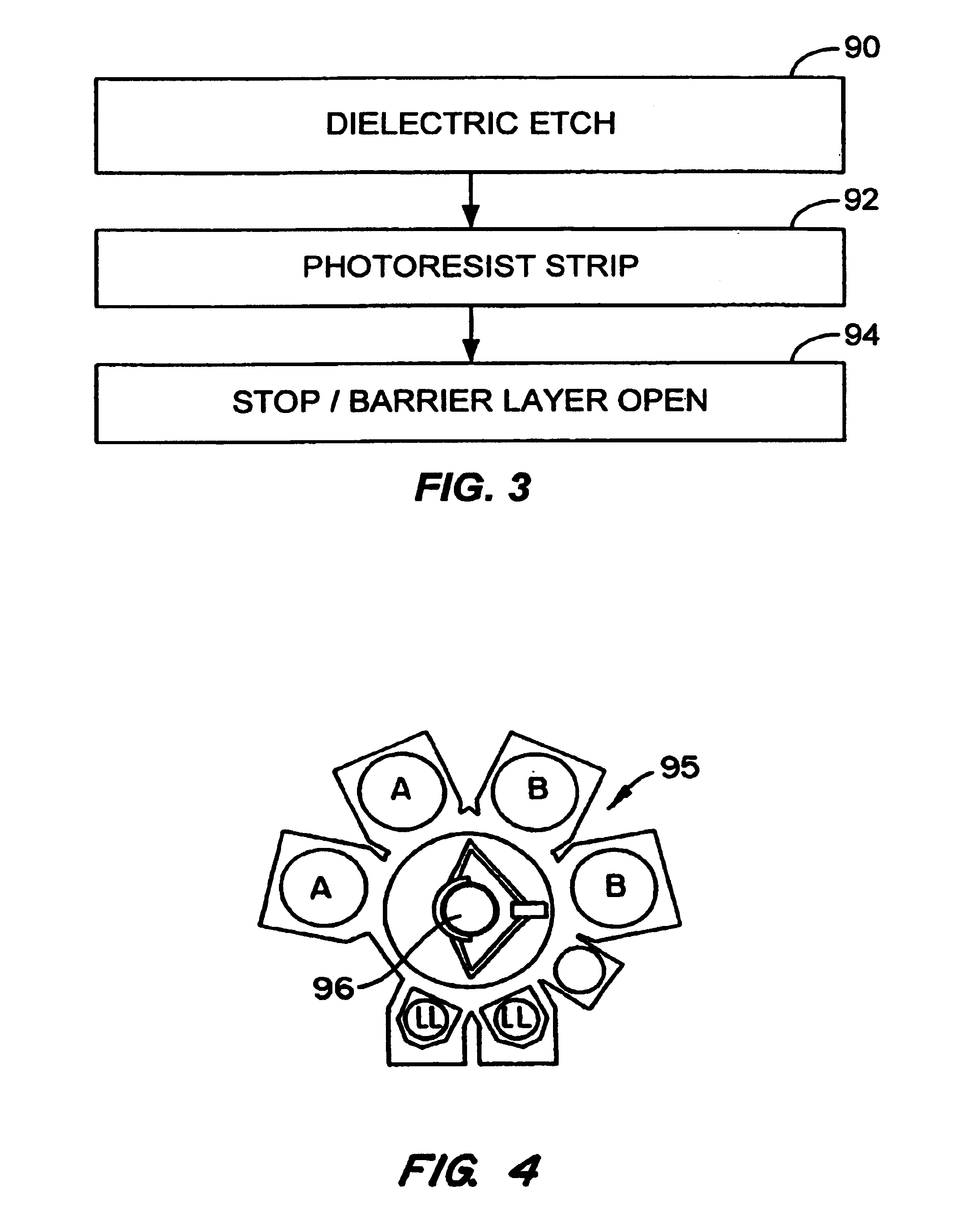
[0090]The first example is particularly useful for a single damascene metal 1 trench etch process. In some applications it is common to form such a single damascene structure for a metal 1 layer before using a dual damascene approach to additional, overlying metal layers. FIG. 6A shows an example of a substrate 200 having a three layer dielectric stack 202 to be etched in step 90. Dielectric stack 205 includes an organic, bottom antireflective coating (BARC) 204, formed over an inorganic, dielectric antireflective coating (DARC) 206, which is formed over a Black Diamond™ layer 208. A deep UV photoresist material 210 is formed over the dielectric stack and a BloK™ layer 212 separates the dielectric stack from the underlying substrate.

[0091]Table 1 set forth below shows the basic steps used to etch the dielectric material, strip the photoresist and open the barrier layer (steps 90, 92 and 94, respectively). As shown in Table 1, step 90 includes two separate steps: a first main etch st...

invention example 2

[0094]The second example is particularly useful for a via etch process such as one used to etch via 222 in substrate 220 shown in FIG. 6B. Substrate 220 includes a BARC layer 224 formed over a DARC layer 226, which is formed over a Black Diamond™228. Layer 228 serves as both the trench and via dielectric layers. A deep UV photoresist material 230 is formed over the dielectric stack and a BloK™ layer 232 separates the dielectric stack from the underlying substrate. A middle stop layer is not included between the trench and dielectric layers as the process relies on the iRM to endpoint the trench etch in a later step.

[0095]This example etches a via in the substrate 220 using a three-step etch process as dielectric etch step 90 that is highly selective to the photoresist and bottom BloK™ layer. In the first step, the BARC layer is etched using a CF4 plasma; the main etch step uses a CHF3 and N2 plasma and the final, over etch step uses a C4F6, O2 and CO plasma. Further details of diele...

invention example 3

[0098]The third example is particularly useful for a dual damascene trench etch process such as one used to etch substrate 240 shown in FIG. 6C. Substrate 240 includes a DARC layer 242 formed over a Black Diamond™ layer 244. The Black Diamond™ layer 244 serves as both the trench and via dielectric layers and does not include a middle stop layer. A deep UV photoresist material 246 is formed over the dielectric stack and a BloK™ layer 248 separates the dielectric stack from the underlying substrate.

[0099]In this example a trench may be etched in substrate 240 using a two step etch process, such as that shown in Table 3 below, as dielectric etch step 90. In the first step, the DARC layer is etched using a CF4 plasma while the main trench etch step uses a CF4, N2 and Ar plasma. The subsequent photoresist strip and stop layer open steps 92 and 94 may use the same parameters as these shown in Table 1 above.

[0100]

TABLE 3PROCESSES CONDITIONS FOR INVENTION EXAMPLE 3ParameterDielectric EtchGa...


PUM

PropertyMeasurementUnit
Temperatureaaaaaaaaaa
Poweraaaaaaaaaa
Poweraaaaaaaaaa

Abstract

An integrated in situ etch process performed in a multichamber substrate processing system having first and second etching chambers. In one embodiment the first chamber includes an interior surface that has been roughened to at least 100 Ra and the second chamber includes an interior surface that has a roughness of less than about 32 Ra. The process includes transferring a substrate having formed thereon in a downward direction a patterned photoresist mask, a dielectric layer, a barrier layer and a feature in the substrate to be contacted into the first chamber where the dielectric layer is etched in a process that encourages polymer formation over the roughened interior surface of the chamber. The substrate is then transferred from the first chamber to the second chamber under vacuum conditions and, in the second chamber, is exposed to a reactive plasma such as oxygen to strip away the photoresist mask deposited over the substrate. After the photoresist mask is stripped, the barrier layer is etched through to the feature to be contacted in the second chamber of the multichamber substrate processing system using a process that discourages polymer formation over the relatively smooth interior surface of the second chamber. All three etching steps are performed in a system level in situ process so that the substrate is not exposed to an ambient between steps. In some embodiments the interior surface of the first chamber has a roughness between 100 and 200 Ra and in other embodiments the roughness of the first chamber's interior surface is between 110 and 160 Ra.

Description

CROSS REFERENCE TO RELATED APPLICATIONS[0001]This application is a continuation-in-part of U.S. application Ser. No. 09 / 538,443, filed Mar. 29, 2000, now U.S. Pat. No. 6,500,357 which claims priority from U.S. Provisional Application No. 60 / 173,412, filed Dec. 28, 1999. This application also claims the benefit of U.S. Provisional Application No. 60 / 365,962, filed Mar. 19, 2002. The Ser. Nos. 09 / 538,443; 60 / 173,412 and 60 / 365,962 applications are incorporated herein by reference.BACKGROUND OF THE INVENTION[0002]The present invention relates to plasma etch processes used in the manufacture of semiconductor integrated circuits. More specifically, the present invention relates to a system level in situ integrated process for etching layered dielectric structures serving as inter-level dielectric layers.[0003]The technology of fabricating semiconductor integrated circuits continues to advance in the number of transistors, capacitors and other electronic devices that can be fabricated on ...

Claims


Application Information

Patent Timeline
IPC IPC(8): H01L21/00H01L21/70H01L21/02H01L21/768H01L21/311
CPCH01J37/32458H01L21/31116H01L21/31138H01L21/67184H01L21/67207H01L21/67219H01L21/6723H01L21/76802H01L21/76804H01L21/76807H01L21/76832H01L21/306
Inventor HSIEH, CHANG-LINMA, DIANA XIAOBINGSHIEH, BRIAN SY YUANYIN, GERALD ZHEYAOSUN, JENNIFERTHACH, SENHLUO, LEEBJORKMAN, CLAES H.
Owner APPLIED MATERIALS INC
Why Eureka
Try Eureka