Semiconductor device and manufacturing method thereof

a technology of semiconductor devices and manufacturing methods, applied in the field of semiconductor devices, can solve problems such as complicated process steps, and achieve the effects of reducing production costs, improving operation characteristics and reliability of semiconductor devices, and reducing power consumption

Inactive Publication Date: 2005-10-04
SEMICON ENERGY LAB CO LTD
View PDF46 Cites 90 Cited by
  • Summary
  • Abstract
  • Description
  • Claims
  • Application Information

AI Technical Summary

Benefits of technology

[0012]The present invention contemplates to provide a technology that solves these problems. In electro-optical devices and semiconductor devices typified by an active matrix liquid crystal device fabricated by using TFTs, the present invention is directed to improve the operation characteristics and reliability of the semiconductor devices and at the same time lower the power consumption, by optimizing the structures of the TFTs employed in various circuits in accordance with the functions of the respective circuits, thereby reducing the production cost and improving the production yield by reducing the number of process steps.
[0013]To accomplish the reduction of the production cost and the improvement of the production yield by reducing the number of process steps, the number of photo-masks used for the fabrication of the TFT must be reduced. In photolithography, the photo-mask is used for forming a resist pattern over the substrate as the mask in the etching process. Therefore, when one photo-mask is used, additional process steps such as resist removing, washing, drying, etc, are necessary before and after the step that uses the photo-mask in addition to the process steps of the film formation and etching. In the photolithography step, too, complicated process steps such as the application of the resist, pre-baking, exposure, development, post-baking, etc, are necessary.

Problems solved by technology

In the photolithography step, too, complicated process steps such as the application of the resist, pre-baking, exposure, development, post-baking, etc, are necessary.

Method used


Image

  • Semiconductor device and manufacturing method thereof
  • Semiconductor device and manufacturing method thereof
  • Semiconductor device and manufacturing method thereof

Examples


embodiment 1

[Embodiment 1]

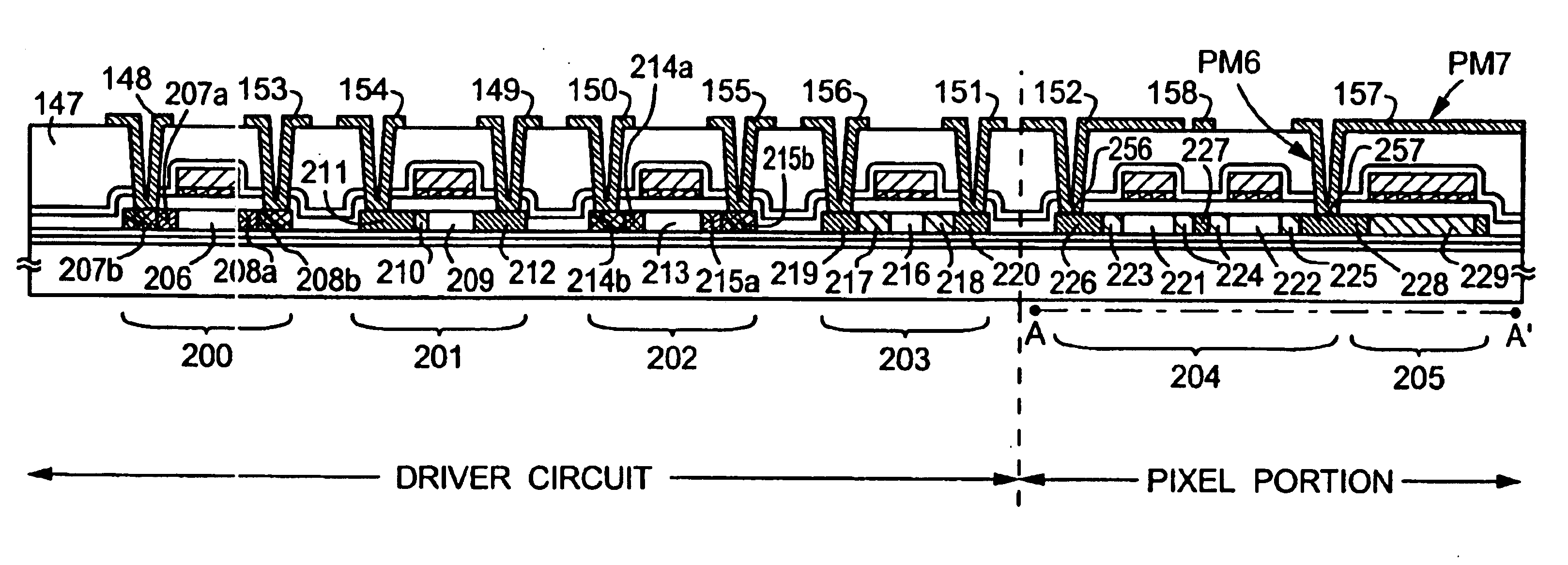
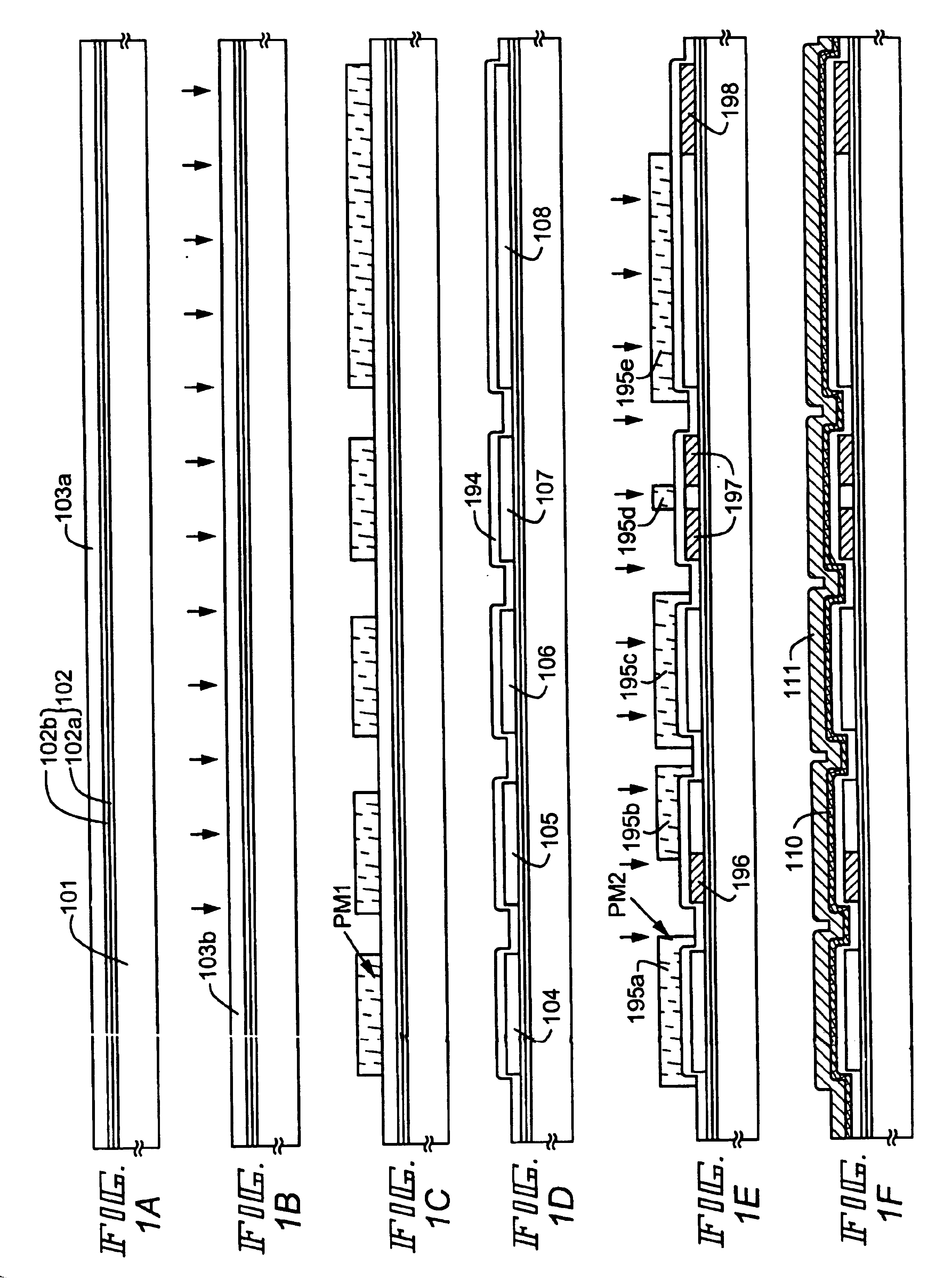
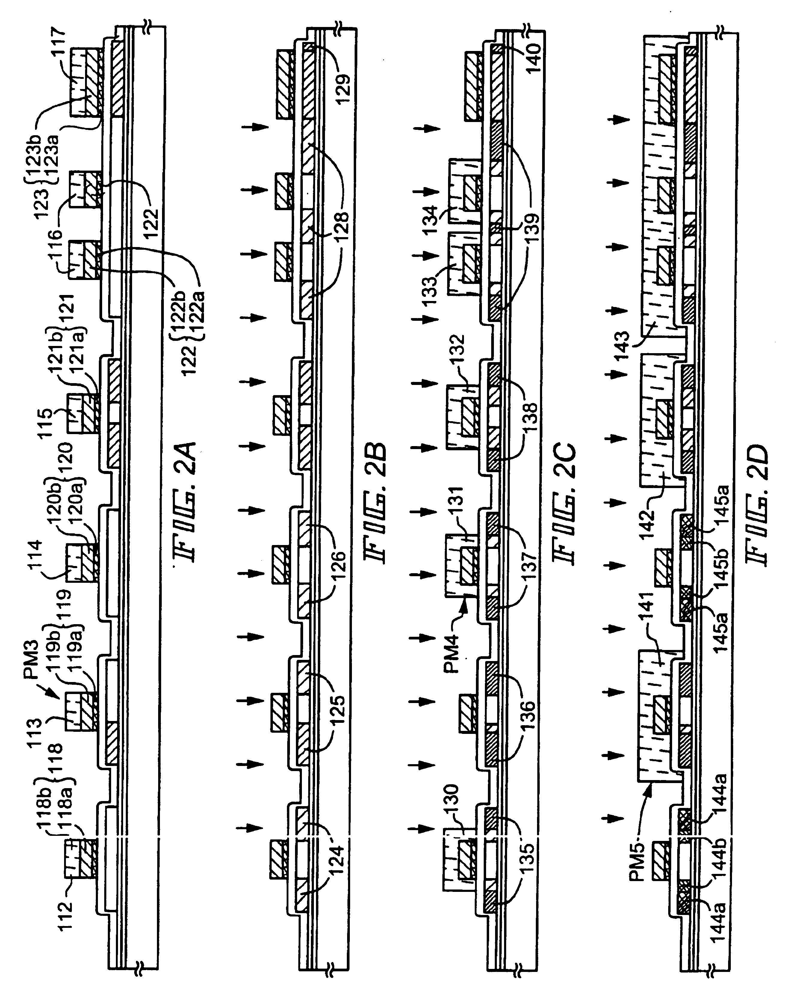
[0052]An embodiment of the present invention will be explained with reference to FIGS. 1A to 3C. In this embodiment, a method of forming simultaneously pixel TFTs and storage capacitors of a pixel section and TFTs of a driving circuit disposed in the periphery of the display region will be explained step-wise in detail.

[0053]In FIG. 1A, as well as barium borosilicate glass or aluminoborosilicate glass as typified by Corning #7059 glass and #1737 glass, plastic substrates which do not have optical anisotropy such as polyethylene terephthatate (PET), polyethylene naphthalate (PEN), polyethersulfone (PES), etc, can be used as the substrate 101. When the glass substrate is used, the substrate may be heat-treated in advance at a temperature lower by about 10 to 20° C. than a glass strain point. A base film 102 of a silicon oxide film, a silicon nitride film or a silicon oxynitride film, etc. is formed on the surface of the substrate 101, on which TFT is to be formed, in ord...

embodiment 2

[Embodiment 2]

[0084]To accomplish a high-precision and high-quality liquid crystal display device, the characteristics of the TFT constituting the each circuit of the pixel TFT and the driving circuit must be improved. One of the required TFT characteristics is the decrease of the current flowing under the OFF state (OFF current) besides the threshold voltage, the field effect mobility, the sub-threshold coefficient (S value), and so forth. When the OFF current value is high, not only the power consumption increases, but also the operation characteristics of the driving circuit get deteriorated and may invite the drop of image quality. In the n-channel TFT fabricated in Embodiment 1, the LDD region is formed, and this LDD region can lower the OFF current value to the extent that renders no problem. On the other hand, since the p-channel TFT has the single drain structure, the increase of the OFF current value often becomes the problem. This embodiment provides a method of fabricatin...

embodiment 3

[Embodiment 3]

[0089]Embodiment 1 showed the example that uses the heat-resistant conductive material such as W and Ta for the gate electrode. The reason why such materials are used is because the impurity elements that are added mainly for valency control are activated by thermal annealing at 400 to 700° C. after the gate electrode is formed. However, such heat-resistant conductive material has the sheet resistivity of about 10 Ω and are not suitable for a liquid crystal display device having a screen size of 4 inches or more. When the gate wiring connected to the gate electrode is made of the same material, the length of the lead wire on the substrate becomes essentially great, and the wiring delay resulting from the influence of the wiring resistance cannot be neglected.

[0090]When the pixel density is VGA, for example, 480 gate wirings and 640 source wirings are formed. When the pixel density is XGA, 768 gate wirings and 1,024 source wirings are formed. As for the screen size of t...


PUM

PropertyMeasurementUnit
glass strain pointaaaaaaaaaa
thicknessaaaaaaaaaa
thicknessaaaaaaaaaa

Abstract

A p channel TFT of a driving circuit has a single drain structure and its n channel TFT, a GOLD structure or an LDD structure. A pixel TFT has the LDD structure. A pixel electrode disposed in a pixel portion is connected to the pixel TFT through a hole bored in at least a protective insulation film formed of an inorganic insulating material and formed above a gate electrode of the pixel TFT, and in an interlayer insulating film disposed on the insulation film in close contact therewith. These process steps use 6 to 8 photo-masks.

Description

BACKGROUND OF THE INVENTION[0001]1. Field of the Invention[0002]This invention relates to a semiconductor device having a circuit comprising thin film transistors (hereinafter referred to as “TFT”) over a substrate having an insulating surface, and a fabrication method thereof. Specifically, the present invention provides a technology that will be appropriately used for an electro-optical device typified by a liquid crystal display device having a pixel section and a driving circuit disposed in the periphery the pixel section, and for an electronic appliance incorporating such an electro-optical device. Note that the term “semiconductor device” used herein represents those devices which operate by utilizing semiconductor characteristics, and embraces within its scope the electro-optical devices as well as the electronic appliances incorporating the electro-optical device that are described above.[0003]2. Description of the Related Art[0004]A technology that uses TFTs for constitutin...

Claims


Application Information

Patent Timeline
Patent Type & Authority Patents(United States)
IPC IPC(8): H01L29/04H01L29/02G02F1/1362H01L21/00G02F1/1368H01L21/60H01L21/77H01L21/84H01L23/552H01L23/60H01L27/12H01L27/146H01L29/786
CPCG02F1/13454H01L27/1248H01L27/12H01L29/78621H01L29/78624H01L27/1222H01L23/552H01L2924/00011H01L2924/07811H01L23/60H01L24/83H01L27/14601H01L2924/01079H01L2224/83851H01L2924/00H01L2924/12042H01L2924/14
Inventor YAMAZAKI, SHUNPEIARAI, YASUYUKIKOYAMA, JUN
Owner SEMICON ENERGY LAB CO LTD
Why Eureka
Try Eureka