Digital-to-analogue converter circuits

a digital-to-analog converter and circuit technology, applied in the field of digital-to-analog converters, can solve the problems of uneconomic supply of a digital-to-analog converter for each channel, flicker noise (sometimes called 1/f noise), and important manufacturing cost, so as to improve the rejection of audio frequency supply ripple, less crosstalk, and chip area saving

Active Publication Date: 2005-10-04
CIRRUS LOGIC INC
View PDF5 Cites 27 Cited by
  • Summary
  • Abstract
  • Description
  • Claims
  • Application Information

AI Technical Summary

Benefits of technology

[0056]The facility to connect the second capacitor of each (say the positive) circuit portion to share charge with the feedback capacitor of either circuit portion enables the second capacitor to in effect be alternately pre-charged to positive and negative (signal dependent) nodes so that, on average, signal dependent loading of a reference source supplying positive and negative (voltage) references to which the second capacitor is connected for charging is mitigated. More particularly, in embodiments each second capacitor is connected alternately to positive and negative signal-dependent nodes of the circuit (in effect to share charge with the feedback capacitors of the positive and negative circuit portions). Still more particularly each second capacitor is connected alternately to positive and negative feedback capacitor (signal) nodes firstly when being charged to the positive reference voltage, and secondly when being charged to the negative reference voltage. Charging each second capacitor to both the positive reference voltage (for two charge-dump cycles) and to the negative reference voltage (for two charge-dump cycles) enables the capacitor to be charged (positively, and negatively) in such a way that the charge can be dumped to positive and negative signal nodes (feedback capacitors), thus facilitating the above-mentioned positive / negative pre-charge. In embodiments this results in an eight phase charge-dump clocking scheme, comprising four successive charge-dump cycles, the second (switched) capacitors being connected to a positive signal node for a first pair of charge-dump cycles and to a negative signal node for a second pair of charge-dump cycles.
[0059]In embodiments this provides additional benefits, of firstly desensitising the output signal to flicker noise of the amplifiers employed, allowing smaller devices to be used therein, with a consequent chip area saving; and secondly improving the rejection of audio frequency supply ripple, giving potentially less crosstalk between DACs, especially when sharing supplies on one chip, or allowing relaxation of the requirements for audio frequency supply decoupling for a given performance, with potential external component cost savings.

Problems solved by technology

However, in such high-volume markets manufacturing cost is also very important.
Furthermore in a stereo or multi-channel system it is often uneconomic to supply a digital-to-analogue converter for each channel with a separate voltage reference supply, or even separate decoupling, PCB traces, or integrated circuit pins.
Two further issues arise with high performance switched-capacitor audio DACs, firstly problems of flicker noise (sometimes called 1 / f noise) in the MOS devices typically used to implement the op amps, and secondly problems with crosstalk between amplifiers due to combinations of common supply impedances, poor audio-frequency supply decoupling, and finite op amp power-supply rejection.
For SNR of 100 dB or greater (120 dB is becoming a target for high-performance systems), it rapidly becomes impractical to achieve a flicker noise corner frequency below say 1 kHz, and even then with a significant impact on chip area and hence cost.
The load regulation bandwidth of active power supplies is often inadequate to prevent millivolts of ripple at higher audio frequencies, especially as these supplies may also be supplying high-power outputs to drive speakers or headphones.
Often several channels of DAC (e.g. six) are implemented on the same silicon chip but without the expense of extra supply pins it is difficult to distribute the supplies to all amplifiers (including power output stages) without several ohms of common supply impedance.

Method used


Image

  • Digital-to-analogue converter circuits
  • Digital-to-analogue converter circuits
  • Digital-to-analogue converter circuits

Examples


Embodiment Construction

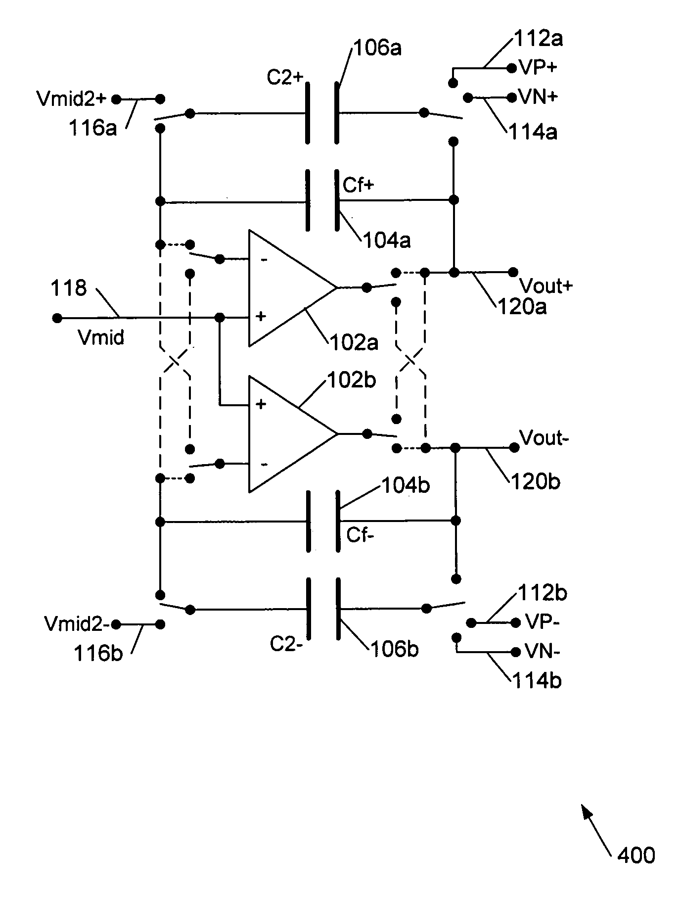
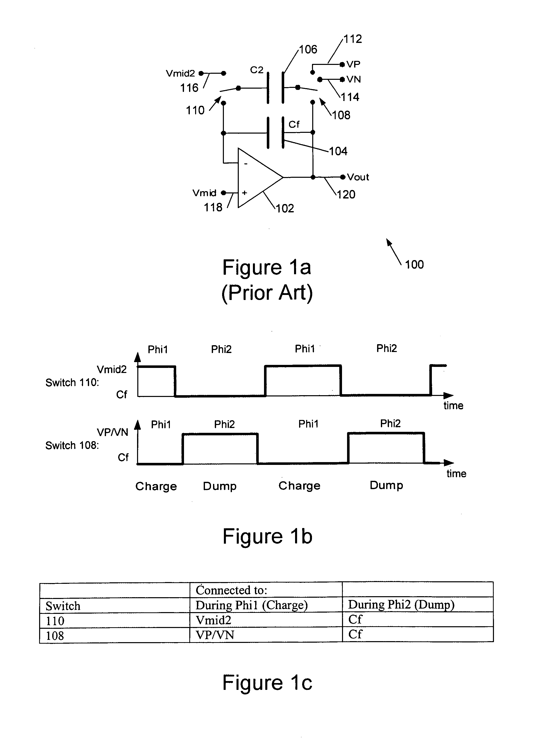
[0073]Referring to FIG. 5a, this shows a differential DAC circuit 500 including chopper switches 501a,b, 502a,b to reduce the signal-dependent reference loading. The DAC circuit of FIG. 5 is a development of that shown in FIG. 2 (like elements are indicated by like reference numerals) and comprises a pair of DAC circuits 500a,b to provide a differential output 520a, b.

[0074]Capacitor 106a is still charged to VP or VN via switches 110a, 108a. However, rather than discharging directly via switches 110a, 108a onto capacitor 104a, it discharges onto either capacitor 104a or 104b, via additional connections 503, 505, and 504, 506, according to the polarity of additional series switches 501a, 502a. There is a similar arrangement for capacitor 106b. The switches 501a, 501b, 502a, 502b may be switched to alternate every cycle giving a 4-phase clocking scheme as shown in Table 5a (below) or every second cycle giving an 8-phase clocking scheme as shown in Table 5c. Other possible clocking sc...


PUM


Abstract

This invention is generally concerned with digital-to-analogue converters and more particularly relates to techniques for reducing signal dependent loading of reference voltage sources used by these converters.A differential switched capacitor digital-to-analogue (DAC) circuit (500) comprises first and second differential signal circuit portions (500a,b) for providing respective positive and negative signal outputs with respect to a reference level, and has first and second reference voltage inputs (112,114) for receiving respective positive and negative references. Each of said first and second circuit portions comprises an amplifier (102a,b) with a feedback capacitor (104a,b), a second capacitor (106a,b), and a switch (108a,b, 110a,b) to switchably couple said second capacitor to a selected one of said reference voltage inputs to charge the second capacitor and to said feedback capacitor to share charge with the feedback capacitor. The switch of said first circuit portion is further configured to connect said second capacitor (106a) of said first circuit portion to share charge with said feedback capacitor (104b) of said second circuit portion; and the switch of said second circuit portion is further configured to connect said second capacitor (106b) of said second circuit portion to share charge with said feedback capacitor (104a) of said first circuit portion. This enables the second capacitors to in effect be alternately pre-charged to positive and negative signal-dependent nodes so that, on average, signal dependent loading of the references is approximately constant.

Description

FIELD OF THE INVENTION[0001]This invention is generally concerned with digital-to-analogue converters and more particularly relates to techniques for reducing signal dependent loading of reference voltage sources used by these converters.BACKGROUND TO THE INVENTION[0002]Digital-analogue conversion based on converting a delta-sigma digital representation of a signal into an analogue waveform is now a commonplace technique. In a simple delta-sigma digital-to-analogue converter a string of pulses is generated, with a pulse density dependent upon the digital value to be converted, and low-pass filtered. The technique is prevalent in many high-volume application areas, for example digital audio, where several channels of high quality relatively low frequency (audio frequency) signals are required. High quality in this context typically implies −100 dB THD (Total Harmonic Distortion) and 100 dB SNR (Signal to Noise Ratio). However, in such high-volume markets manufacturing cost is also ve...

Claims


Application Information

Patent Timeline
Patent Type & Authority Patents(United States)
IPC IPC(8): H03M3/00H03M3/02H03M1/66
CPCH03M3/322H03M3/502H03M3/02
Inventor FRITH, PETER J.PENNOCK, JOHN L.
Owner CIRRUS LOGIC INC
Why Eureka
Try Eureka