Light-emitting diode encapsulation material and manufacturing process

a technology of encapsulation material and light-emitting diodes, which is applied in the direction of photomechanical equipment, instruments, and semiconductor/solid-state device details, etc., can solve the problems of inability to increase the speed of producing light-emitting diodes, inefficient production, and internal stress between epoxy resins, etc., to achieve rapid curing, enhance production efficiency, and cure rapid

Inactive Publication Date: 2005-10-25
YANG YUNG SHU
View PDF4 Cites 33 Cited by
  • Summary
  • Abstract
  • Description
  • Claims
  • Application Information

AI Technical Summary

Benefits of technology

[0014]Specifically, the present invention provides encapsulation material and manufacturing processes of a light-emitting diode, wherein comprises a photo-sensitive polymer constituting at least one of an Oligomer or a reactive Monomer, and a Photoinitiator. After a LED chip encapsulation, the photo-sensitive polymer is exposed to visible light or ultraviolet light irradiation, or electron beam, free of infrared rays, thereby triggering a free radical polymerization reaction of the fluid photo-sensitive polymer, and rapid curing thereof under room temperature, eliminating the need for baking during encapsulation manufacturing process of the light-emitting diode, while prompting rapid curing thereof, and thereby enhancing production efficiency.
[0015]Another objective of the present invention is to provide encapsulation material and manufacturing processes of the light-emitting diode wherein comprises the photo-sensitive polymer constituting at least one of an Oligomer or a reactive Monomer. After a LED chip encapsulation, irradiation with an electron beam is carried out, whereby electron bombardment is utilized to accomplish amalgamation of material molecules, thereby triggering free radical polymerization reaction of the fluid photo-sensitive polymer, and rapid curing thereof under room temperature, eliminating the need for baking during encapsulation manufacturing process of the light-emitting diode, while prompting rapid curing thereof, and thereby enhancing production efficiency.
[0016]Furthermore, when implementing the present invention, a Silane coupling agent may be added to the encapsulant material, thereby increasing the bonding strength among between the materials; an ultraviolet absorber may be added to increase resistance against ultraviolet light degradation; a Hindered Amine Light Stabilizer may be added to avoid free radical chemistry structure destruction.

Problems solved by technology

Furthermore, because of an enormous discrepancy between thermal expansion coefficients of the epoxy resin and the LED chips, during process of curing, cooling and shrinkage of the epoxy resin, internal stress may occur between the epoxy resin and the LED chips, engendering cracking of the epoxy resin, fracturing of the LED chips, separation of adhesion, shifting or splitting of component connected Leadframes, etc.
From the aforementioned integral manufacturing process of the light-emitting diode, wherein an extremely long time is spent in encapsulation of the epoxy resin and heat baking, furthermore, component formulation is complicated, and thus results in an inability to increase speed of producing the light-emitting diode, resulting in inefficient production.

Method used


Image

  • Light-emitting diode encapsulation material and manufacturing process
  • Light-emitting diode encapsulation material and manufacturing process
  • Light-emitting diode encapsulation material and manufacturing process

Examples


Embodiment Construction

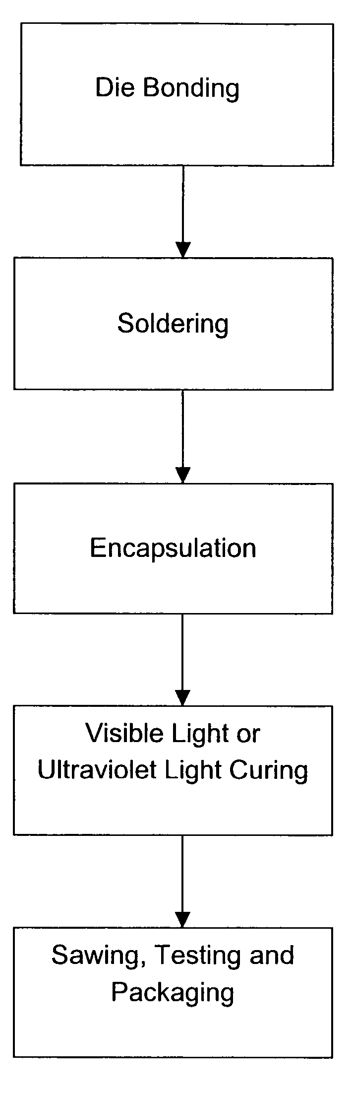
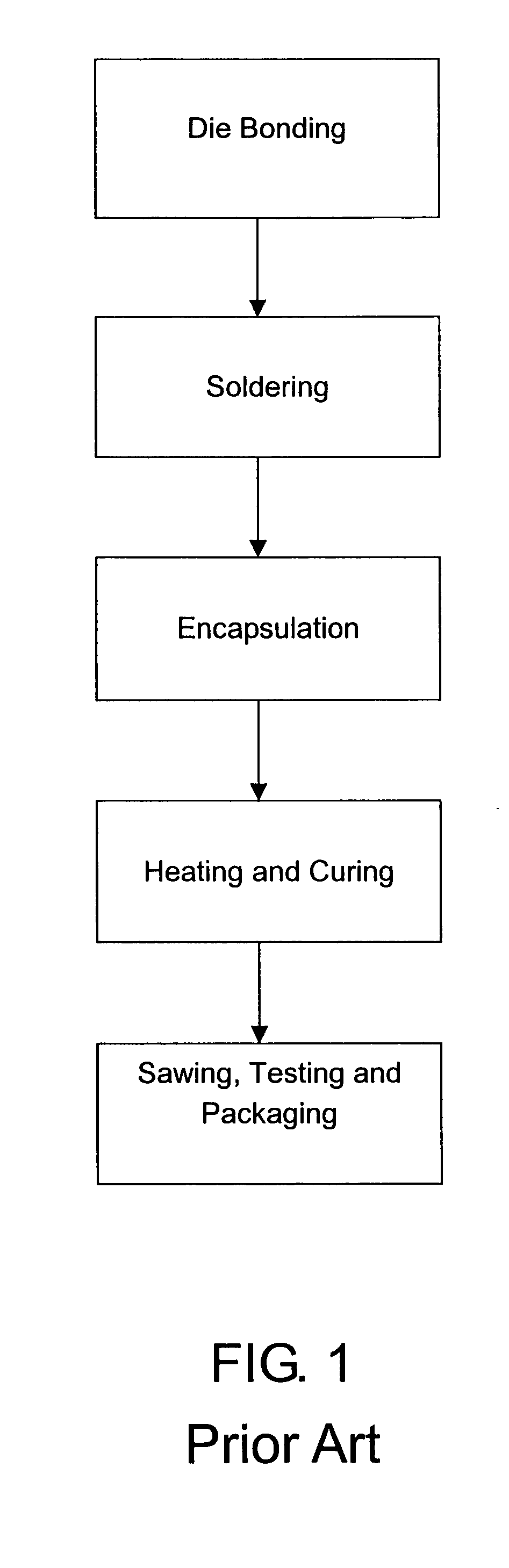
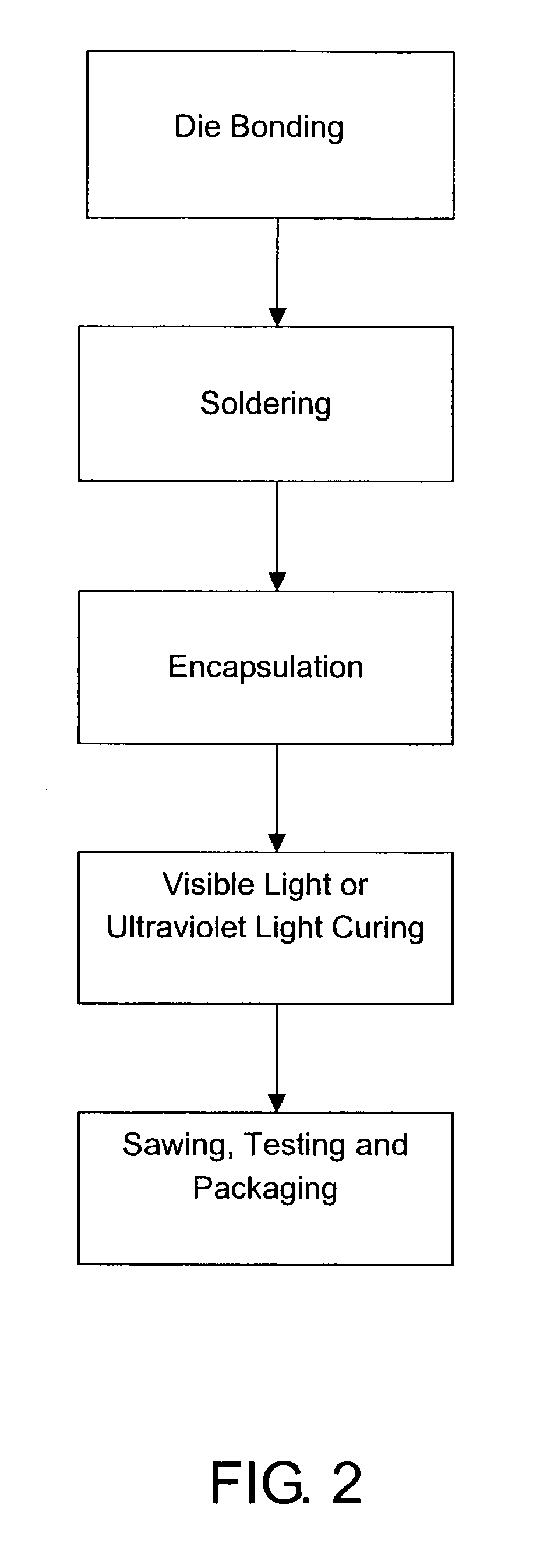
[0022]Referring to FIG. 2, which shows encapsulation material and manufacturing process for a light-emitting diode according to the present invention, wherein an integral manufacturing process of the light-emitting diode is divided into steps as disclosed hereinafter:

[0023]1, Die Bonding: The light-emitting diode crystalline grains LED chip is placed onto a pre-punched first leadframe.

[0024]2, Soldering: A metal lead is made to connect the light-emitting diode Chip and a second lead stand thereby allowing conductance therethrough, enabling the first leadframe, a second leadframe, and the light-emitting diode chip to form an electrical link thereof.

[0025]3, Encapsulation: Upon injecting a thick, viscous, fluid photosensitive polymer into a mold, place the light-emitting diode LED chip, the first leadframe and the second leadframe into the mold.

[0026]4. Curing: Upon encapsulation, the photosensitive resin is exposed to visible light or ultraviolet light or electron beam, allowing prom...


PUM

PropertyMeasurementUnit
timeaaaaaaaaaa
timeaaaaaaaaaa
photosensitiveaaaaaaaaaa

Abstract

A light-emitting diode (LED) encapsulation material and manufacturing process comprising a photo-sensitive polymer constituting at least one of an Oligomer or a reactive Monomer, and a Photoinitiator. After a LED chip encapsulation, the photo-sensitive polymer is exposed to visible light or ultraviolet light, or electron beam, free of infrared rays, thereby triggering a free radical polymerization reaction of the photo-sensitive polymer, and rapid curing thereof under room temperature, eliminating the need for heating in a furnace during encapsulation manufacturing process of the light-emitting diode, while prompting rapid curing thereof, and thereby enhancing production efficiency.

Description

BACKGROUND OF THE INVENTION[0001](a) Field of the Invention[0002]The present invention primarily relates to an application of encapsulation material and manufacturing processes of a light-emitting diode (LED), eliminating the need for heating in a furnace during encapsulation manufacturing process of the light-emitting diode, prompting rapid curing thereof, and thereby enhancing production efficiency.[0003](b) Description of the Prior Art[0004]Referring to FIG. 1, which shows a manufacturing process of a traditional light-emitting diode (LED), whereby the manufacturing process is divided into the following steps:[0005]1, Die Bonding: The light-emitting diode chip is placed and bonded onto a pre-punched first leadframe.[0006]2, Soldering: A metal lead is made to connect the light-emitting diode chips and a second lead stand thereby allowing conductance therethrough, enabling the first leadframe, a second leadframe, and the light-emitting diode chips to form an electrical link thereof...

Claims


Application Information

Patent Timeline
Patent Type & Authority Patents(United States)
IPC IPC(8): H01L21/00H01L33/00G03F7/00H01L21/56H01L33/56H01L33/62
CPCG03F7/0005H01L21/56H01L33/52H01L33/56H01L2924/0002H01L2924/00D03D13/004D03D15/00D06M15/21D10B2505/18
Inventor YANG, YUNG-SHU
Owner YANG YUNG SHU
Why Eureka
Try Eureka