Transparent board with conductive multi-layer antireflection films, transparent touch panel using this transparent board with multi-layer antireflection films, and electronic equipment with this transparent touch panel

a technology of anti-reflection films and transparent boards, applied in the direction of instruments, static indicating devices, optical elements, etc., can solve the problems of plastic base showing difficulty in transmitting the transmissivity in comparison with glass base, glass substrate has a drawback of fragility and weight, and the conductivity of plastic base is reduced on the most exterior surface, so as to reduce optical wave interference, high transmission, and high transmission

Inactive Publication Date: 2005-10-25
PANASONIC CORP +1
View PDF22 Cites 49 Cited by
  • Summary
  • Abstract
  • Description
  • Claims
  • Application Information

AI Technical Summary

Benefits of technology

[0007]To solve the problems above described, the present invention is to offer a transparent electrically conductive baseboard with antireflection multi-layer transparent films on a transparent substrate that are first, second and third-layer thin films with thickness optically considering the refraction index of the substrate, while the transparent substrate has a refraction index ranging from 1.48 through 1.70 and the first transparent dielectric film on the substrate has the higher refraction index ranging from 1.50 through 2.50 and the second film has the lower refraction index ranging 1.35 through 1.60 and the most exterior third transparent film has electrical conductivity. The present invention provides high transmission by reducing the optical waves interference with the described multi-layer thin films.
[0008]Furthermore, to solve the problems above described, the present invention is to offer a transparent touch panel including a transparent fix board with the third conductive layer and a transparent flexible board with the third conductive layer situated separately from the fix board that are electrically connected to an external circuit at the third layer of conductive transparent film, whose first transparent film layer has refraction index of 1.50 through 2.50 which is higher than the selected transparent fix substrate and / or flexible transparent substrate, and the second layer has refraction index of 1.35 through 1.60 which is lower than the selected transparent fix substrate and / or flexible transparent substrate. The present invention provides high transmission by reducing the optical waves interference with the described multi-layer thin films.

Problems solved by technology

However, the glass substrate has a drawback of fragility and big weight, therefore light and no fragile transparent plastic substrate is recently used to form the multi-layer films.
Therefore the plastic base still showed difficulty for the transmissivity in comparison with glass base.
Again, although multi-layer films with antireflection coating of transparent dielectric thin films are effective to improve transmissivity, the coating on the most exterior surface reduces the conductivity of the surface.
This idea has drawback that the thickness of the second layer is restricted by the thickness of the third-layer, which may prevent high transmissivity.

Method used


Image

  • Transparent board with conductive multi-layer antireflection films, transparent touch panel using this transparent board with multi-layer antireflection films, and electronic equipment with this transparent touch panel
  • Transparent board with conductive multi-layer antireflection films, transparent touch panel using this transparent board with multi-layer antireflection films, and electronic equipment with this transparent touch panel
  • Transparent board with conductive multi-layer antireflection films, transparent touch panel using this transparent board with multi-layer antireflection films, and electronic equipment with this transparent touch panel

Examples


embodiment 1

[0022]Conductive multi-layer antireflection films in Embodiment 1 is explained in the following using the figures.

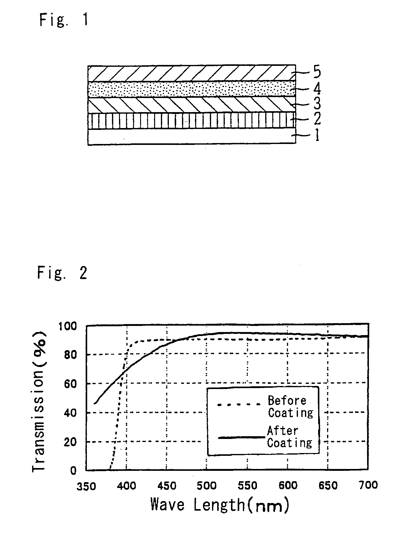
[0023]FIG. 1 is an outline of the idea to configure conductive multi-layer antireflection films in Embodiment 1.

[0024]1 is the transparent substrate. The substrate 1 is sufficient at ordinary obtainable quality with refraction index ranging from 1.48 through 1.7. For example, optically transparent substrates are available such as glass with refraction index 1.48–1.70, polycarbonate with refraction index 1.59, polyethylene terephthalate with refraction index 1.66.

[0025]2 is a thin film on the substrate 1 that is formed before multi-layer thin films are laid. This thin film 2 is coated before laying multi-layer thin films in order to harden the surface of the substrate 1 for protection against scratches and the like, and to make the multi-layer thin films stick closely on the substrate 1, which is called “undercoat” in the following. Generally, the undercoat adopts a hard ...

example 1

[0042]A polycarbonate hard-coated substrate with refraction index 1.59 is prepared and the surface is cleaned with supersonic washer. The substrate is set in vacuum evaporation equipment after drying, and then air is discharged. The equipment is heated up to 130 centigrade Celsius with micro heater and halogen heater until the film is fully grown on the substrate and air is leaked. The micro heater and the halogen heater both heat up the substrate. The chemical substance should be prepared for growth of the first-, the second-, and the third-layer thin films.

[0043]One hour after the heating is started, film growth is begun. The first-layer thin film on the hard-coat surface as undercoating is grown of main component ZrO2 using chemical substance (ZrO2 tablet, made by Optron Co., product) prepared in the equipment. The time for deposition is set 3 minutes 30 second and the film thickness is set 140 nm. Next step grows the second-layer thin film onto the first-layer film with main com...

example 2

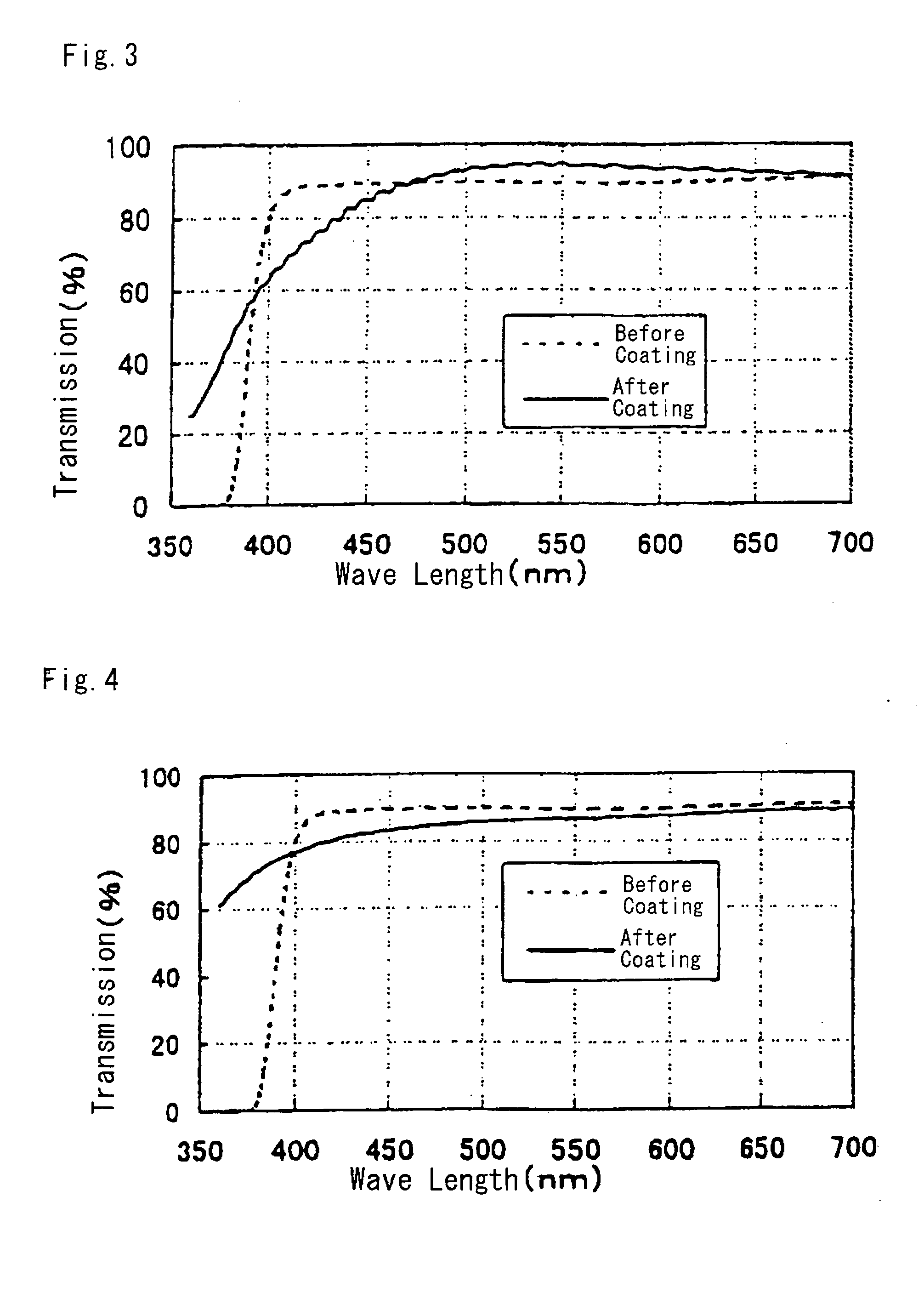
[0046]A polycarbonate hard-coated substrate exactly the same as Example 1 is set in the vacuum evaporation equipment and the first-layer thin film of main component TiO2 is grown. The time for deposition was 4 minutes and the thickness was 65 nm. Then the second-layer thin film of main component SiO2 is grown with thickness of 115 nm. The third-layer thin film is grown of main component ITO with thickness of 30 nm. FIGS. 3 and 12 show the transmissivity of the conductive multi-layer antireflection films above obtained, which presents a peak at 540 nm of wavelength and 94.5% of transmissivity at 550 nm of wavelength and 93.5% of view-sense transmission. It presents 550 Ω / □ of surface resistance.


PUM

PropertyMeasurementUnit
refractive indexaaaaaaaaaa

Abstract

With objectives of providing a transparent board with conductive multi-layer antireflection, under condition of high transmissivity not only on a glass substrate but also on a non-glass transparent substrate with property of conductivity and demanded resistance at most exterior surface, laminating at least three layer thin films on a transparent substrate provides with an effect of high transmissivity by suppressing reflection from interference of optical waves, in which the transparent first dielectric layer thin film on the substrate that has a higher refractive index than the substrate has, the transparent second dielectric layer thin film next to the first-layer film that has a lower refractive index than the substrate has, and the most exterior transparent third conductive-layer thin film.

Description

FIELD OF THE INVENTION[0001]The present invention relates to a transparent board with conductive multi-layer antireflection films, in further details, relates to a transparent touch panel using this transparent board with multi-layer antireflection films and electronic equipment with this transparent touch panel.BACKGROUND OF THE INVENTION[0002]At present, it is known that electrodes for photoelectric transducers such as solar batteries, displaying devices of liquid crystals, and electrodes for touch panels are made using a transparent conductive film of indium tin oxide (ITO: In2O3+SnO2) or tin oxide (SnO2) formed on a transparent substrate such as glass. Especially for use in liquid crystal or electrodes for touch panels, high transmissivity in visible wavelength and optimum surface resistance are demanded. Many studies are made using the glass substrates and resulted in many inventions of multi-layer films that present high transmissivity and optimum surface resistance. However, ...

Claims


Application Information

Patent Timeline
Patent Type & Authority Patents(United States)
IPC IPC(8): G02B1/11G02B1/10G06F3/033H01H13/70H01H13/702G02F1/1335G02F1/13
CPCG02B1/116G06F3/033H01H13/702G02F1/133502H01H2209/014H01H2209/082H01H2231/004G02F2201/38
Inventor FUKUI, TOSHIHARUNAKANISHI, AKIRAMOROI, HIROSHIKATSURAGAWA, JUN
Owner PANASONIC CORP
Why Eureka
Try Eureka