

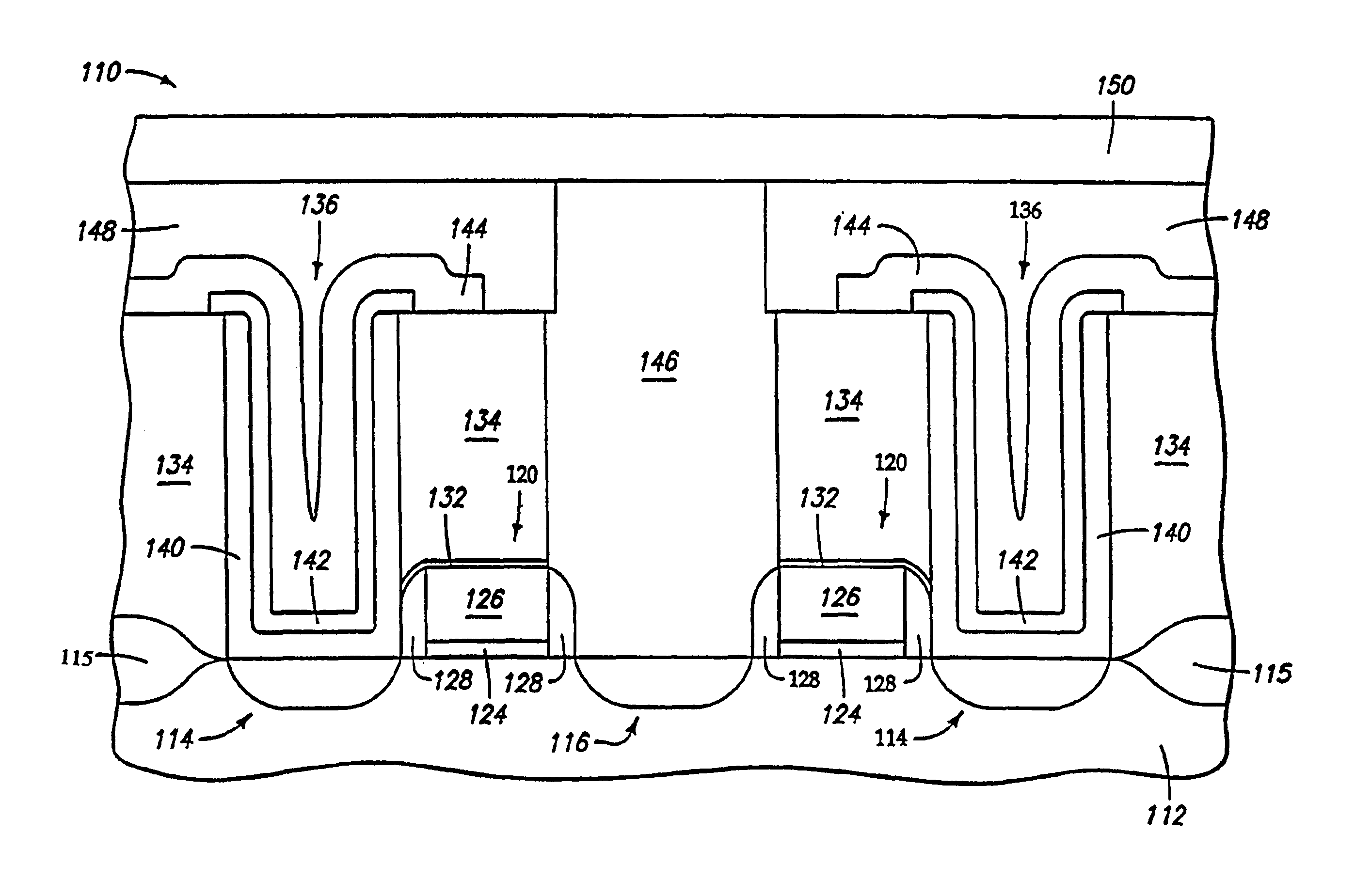
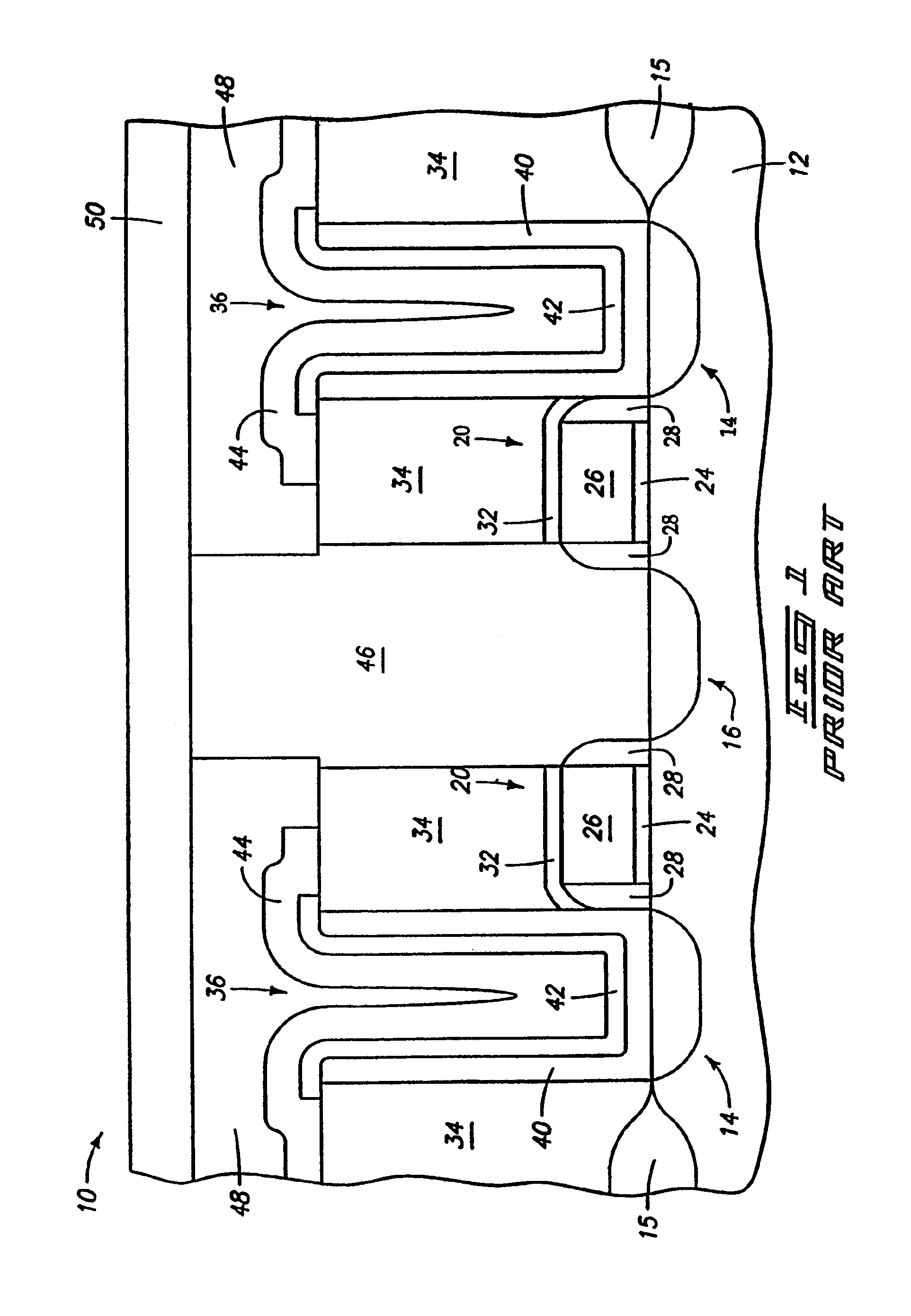
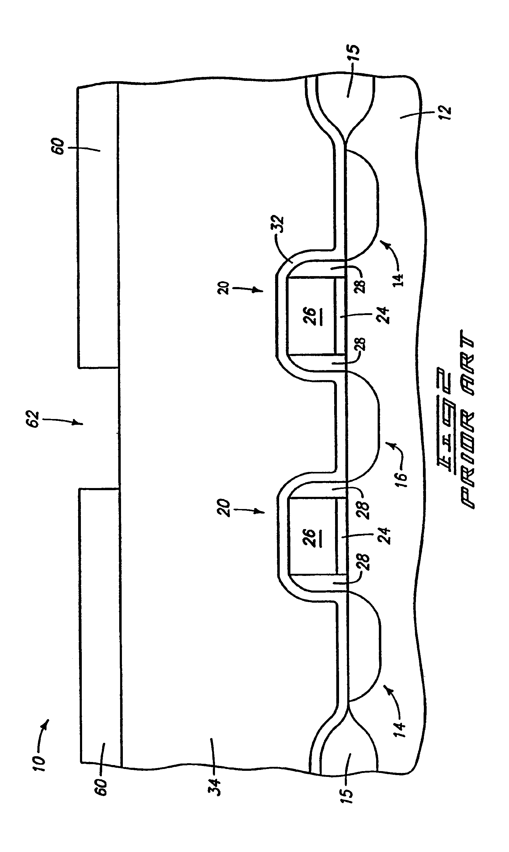
Films doped with carbon for use in integrated circuit technology
a technology of integrated circuit technology and carbon film, applied in the field of films, can solve the problems of poor selectivity of art selective etching methods, constant risk of protective materials being etched away completely, and less selectivity when, so as to achieve the effect of improving capacitive characteristics and reducing the dielectric constan
- Summary
- Abstract
- Description
- Claims
- Application Information
AI Technical Summary
Benefits of technology
Problems solved by technology
Method used
Image

Examples
example 1
[0068]An etch-resistant film was prepared in a chemical vapor deposition reactor under the following conditions: a pressure of about 500 mTorr, a temperature of about 575° C., an N2O flow rate of about 50 sccm, an O2 flow rate of about 50 sccm, and a BTBAS flow rate of about 125 sccm. The resulting film had a stoichiometric composition of SiO1.4N0.2C0.1, and a thickness of about 1040 angstroms.
example 2
[0069]An etch-resistant film was prepared in a chemical vapor deposition (CVD) reactor under the following conditions: a pressure of about 500 mTorr, a temperature of about 575° C., an N2O flow rate of about 150 sccm, and a BTBAS flow rate of about 125 sccm. The resulting film had a stoichiometric composition of SiO1.3N0.5C0.3 and a thickness of about 630 angstroms.
PUM
| Property | Measurement | Unit |
|---|---|---|
| thicknesses | aaaaa | aaaaa |
| thickness | aaaaa | aaaaa |
| dielectric constant | aaaaa | aaaaa |
Abstract
Description
Claims
Application Information