
Organic light emitting devices based on the formation of an electron-hole plasma

a light-emitting device and electron-hole plasma technology, applied in the direction of discharge tube luminescnet screen, active medium material, semiconductor lasers, etc., can solve the problem of limiting quantum efficiency, singlet-polaron quenching limits the quantum efficiency, and the highest efficiency of organic electroluminescence is typically realized

Inactive Publication Date: 2005-11-29
THE TRUSTEES FOR PRINCETON UNIV
View PDF13 Cites 24 Cited by
  • Summary
  • Abstract
  • Description
  • Claims
  • Application Information

AI Technical Summary

Benefits of technology

[0020]In a gateless embodiment, the organic layer can be disposed on a layer of high band-gap material that has a band-gap that is higher than the band gap of the organic layer and a nominal index of refraction that is less than the ...

Problems solved by technology

However, the highest efficiency organic electroluminescence is typically realized at low current densities because non-radiative losses increase under high injection.
At the excitation densities required for electrically-pumped lasing, such losses might render organic lasers impractical.
In amorphous films, triplets induce losses that can be minimized by high rates of triplet-triplet and triplet-polaron annihilation, and in films that employ Förster energy transfer between host and guest molecules, singlet-polaron quenching limits the quantum efficiency.
The bulk tetracene crystals used in this device possess low optical confinement making it difficult to account for the observation of spectral narrowing at the reported threshold current density.
The device of Schön, however, does not teach or suggest the formation of an EHP within the device.

Method used


Image

  • Organic light emitting devices based on the formation of an electron-hole plasma
  • Organic light emitting devices based on the formation of an electron-hole plasma
  • Organic light emitting devices based on the formation of an electron-hole plasma

Examples


Embodiment Construction

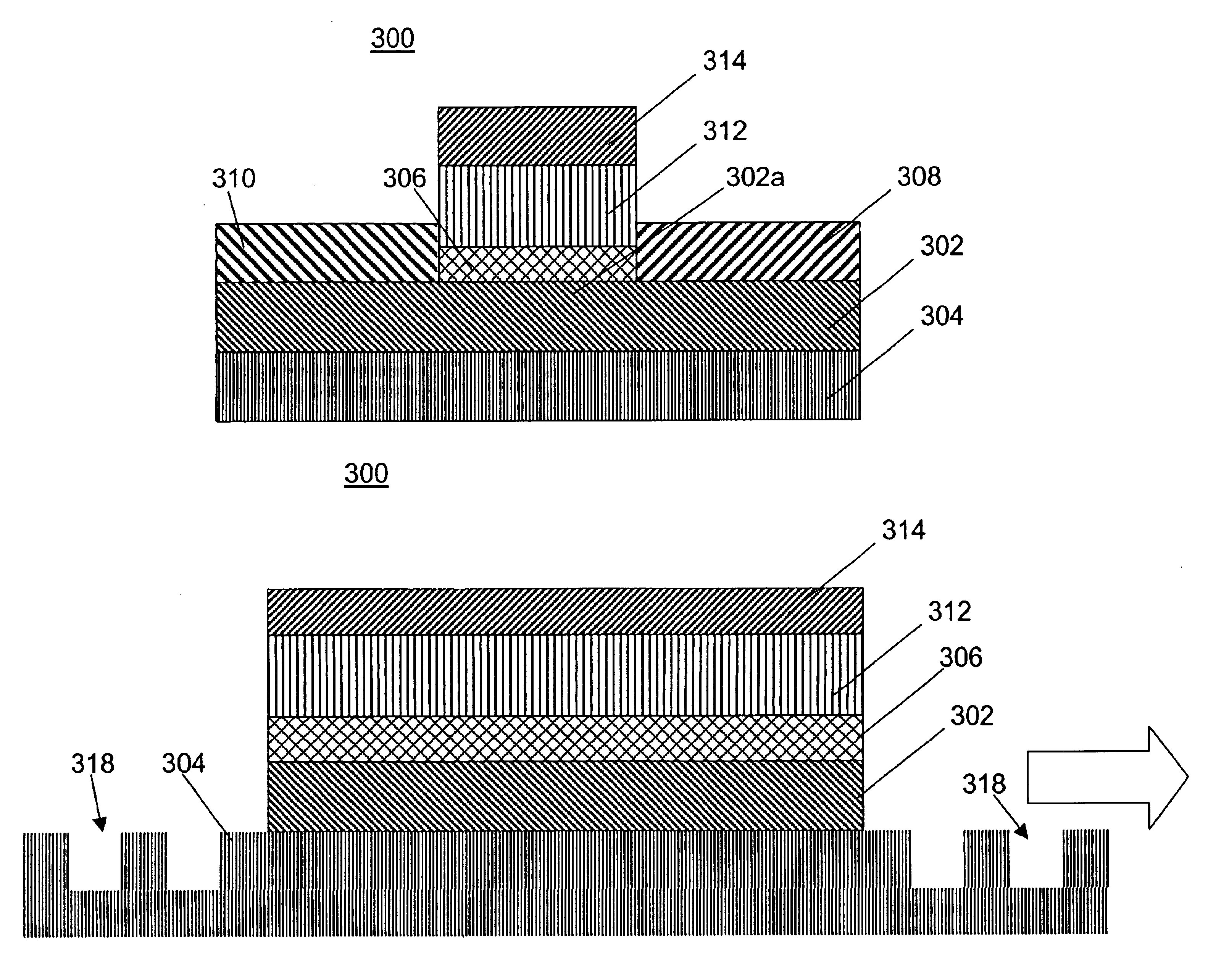
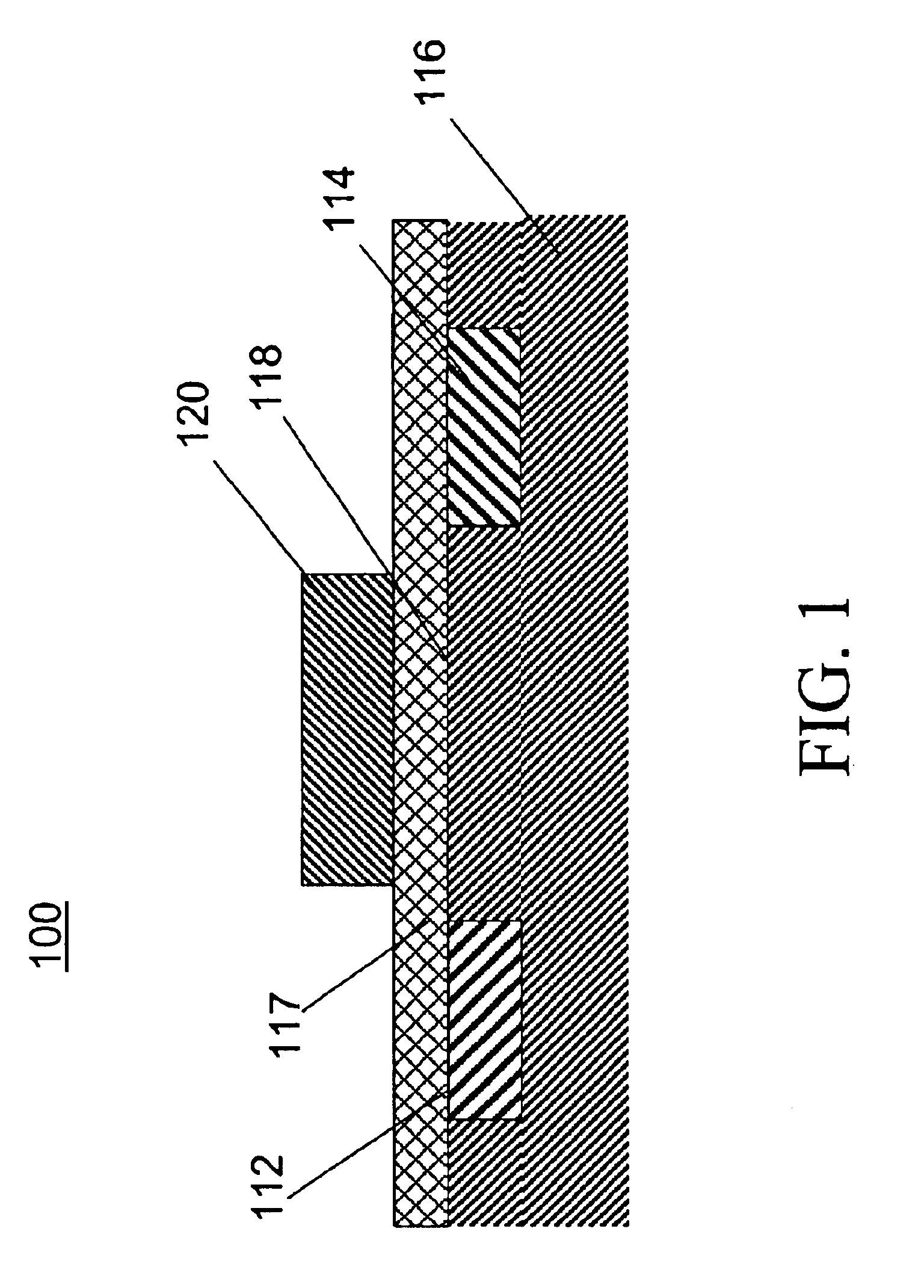
[0039]Generally, devices according to the invention exploit the formation of an electron-hole plasma (EHP) within an organic layer of the device. The embodiments disclosed herein provide technologically applicable structures based preferably on crystalline or amorphous organic thin films or polymers that maximize electrical (i.e., carrier) confinement, optical (i.e., modal) confinement, and photon confinement (i.e., feedback) in the device.

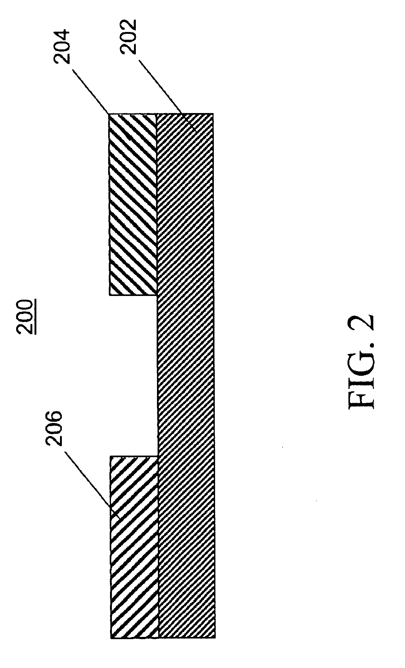
[0040]FIG. 2 depicts a light emitting device 200 according to the invention. As shown, the device 200 includes an organic thin film layer 202, having a preferred thickness on the order of about 50 nm. Typical dimensions for a device according to the invention are 5 mm×5 mm, although smaller devices, such as 0.5 mm×0.5 mm, are possible. The device also includes a first electrical contact 204 that is adapted to inject electrons into the organic layer 202, and a second electrical contact 206 that is adapted to inject holes into the organic layer 202....


PUM


Abstract

When the density of excitons in an organic single crystal (including the linear acenes, polyacenes, and thiophenes) approaches the density of molecular sites, an electron-hole plasma may form in the material altering the overall excitonic character of the system. The formation of the electron-hole plasma arises as a result of the screening of Coulomb interactions within individual excitons by injected free carriers. The large exciton densities required to accomplish this screening process can only be realized when excitons collect near dislocations, defects, traps, or are confined in heterostructures. Such confinement and subsequently large exciton densities allows for the observation of physical phenomena not generally accessible in an organic material. Specifically, the formation of an electron-hole plasma in an organic single crystal can allow for the observation of field-effect transistor action and electrically-pumped lasing. Amorphous organic materials and polymeric organic materials can also used to sustain an electron-hole plasma and demonstrate similar phenomena as well.

Description

GOVERNMENT RIGHTS[0001]This invention was made with Government support under one or more contracts. The government may have rights in this invention.RESEARCH AGREEMENTS[0002]The claimed invention was made by, on behalf of, and / or in connection with one or more of the following parties to a joint university-corporation research agreement: Princeton University, The University of Southern California, and the Universal Display Corporation. The agreement was in effect on and before the date the claimed invention was made, and the claimed invention was made as a result of activities undertaken within the scope of the agreement.FIELD OF THE INVENTION[0003]This invention relates to organic light emitting devices. More particularly, the invention relates to organic light emitting devices having compositions and geometries that are suitable to provide lasing based on the formation of an electron hole plasma within the device.BACKGROUND OF THE INVENTION[0004]Recent reports of electrically-pump...

Claims


Application Information

Patent Timeline
IPC IPC(8): H01L51/50H01S5/12H01S5/125H01S5/20H01S5/36
CPCH01S5/36H01S5/06203H01L51/006H01L51/5048H01L51/5296H01S5/12H01S5/125H01S5/2004H10K85/633H10K50/14H10K50/30
Inventor HOLMES, RUSSELL JAMES DELMARBALDO, MARC A.FORREST, STEPHEN R.
Owner THE TRUSTEES FOR PRINCETON UNIV
Learn More