

Thin-film semiconductor device and method of manufacturing the same
a technology of thin film and semiconductor, applied in semiconductor devices, semiconductor/solid-state device details, electrical equipment, etc., can solve the problems of ineffective use of limited resources, most parts are ground and wasted, and the normal semiconductor chip itself has no flexibility
- Summary
- Abstract
- Description
- Claims
- Application Information
AI Technical Summary
Benefits of technology
Problems solved by technology
Method used
Image

Examples
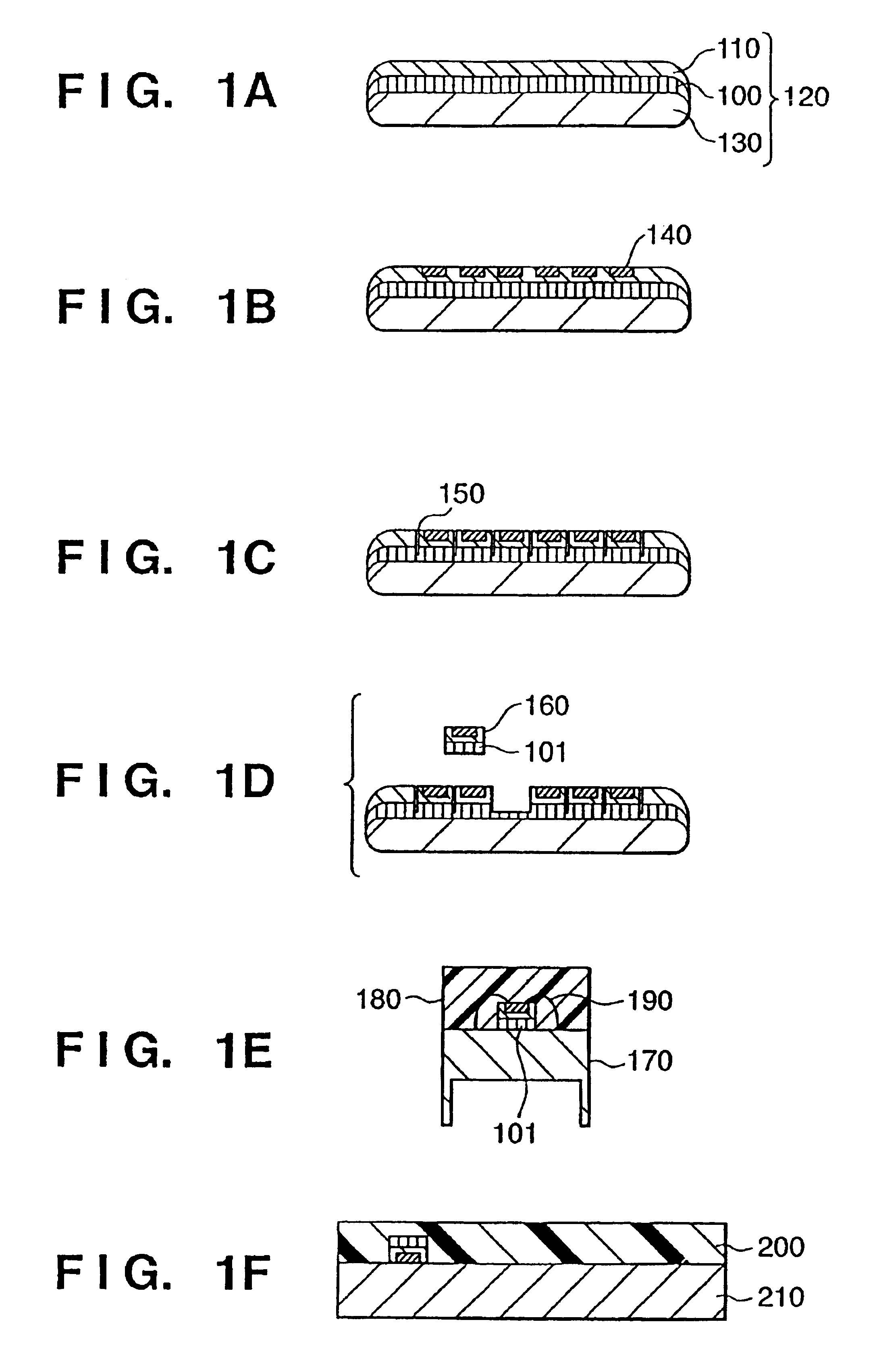
example 1
[0052]A p-type single-crystal Si substrate having a resistivity of 0.01 Ω·cm was prepared. The substrate surface was anodized in an HF solution. The anodizing conditions were
[0053]Current density: 7 (mA·cm−2)
[0054]Anodizing solution: HF:H2O:C2H5OH=1:1:1
[0055]Time: 11 (min)
[0056]Thickness of porous Si layer: 12 (μm)
[0057]The porosity of the porous Si layer was adjusted such that a high-quality epitaxial Si layer could be formed on the porous Si layer and the porous Si layer could be used as a separation layer. More specifically, the porosity was 20%. The thickness of the porous Si layer is not limited to the above thickness and may be several hundred μm to 0.1 μm. The type of the single-crystal Si substrate is not limited to the p type and may be n type. The resistivity of the substrate is not limited to the particular value. The substrate typically has a resistivity ranges from 0.001 to 50 Ω·cm, preferably from 0.005 to 1 Ω·cm, and more preferably from 0.005 to 0.1 Ω·cm.
[0058]This s...
example 2
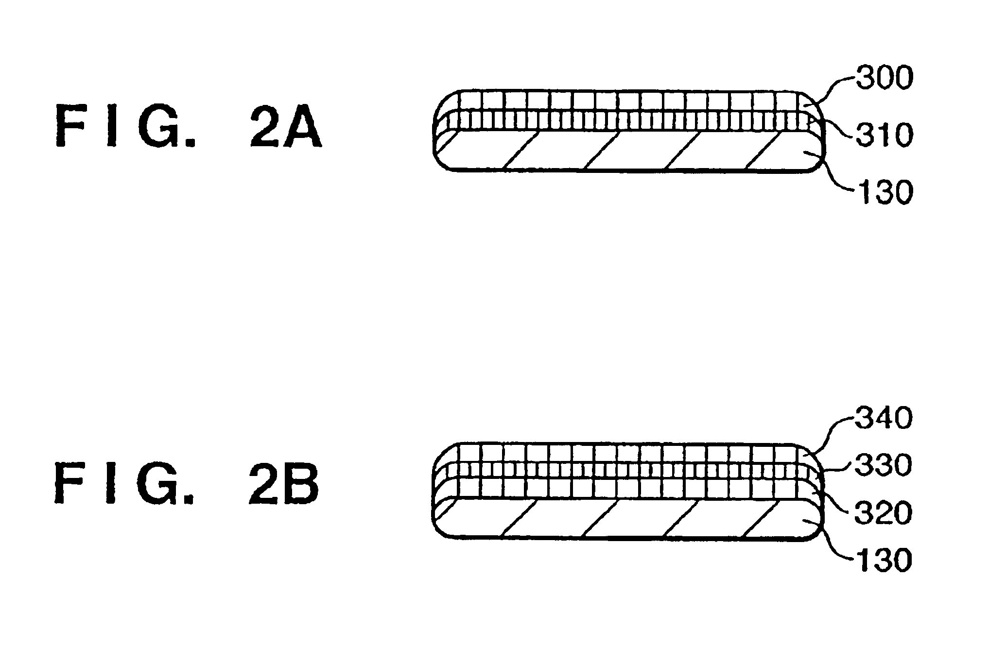
[0076]In Example 1, a single porous layer was used. In Example 2, two porous layers having different porosities were formed.
[0077]First, the surface of a silicon substrate was anodized under the following conditions.
[0078]Current density: 8 (mA·cm−2)
[0079]Anodizing solution: HF:H2O:C2H5OH=1:1:1
[0080]Time: 5 (min)
[0081]Thickness of porous Si layer: 6 (μm)
[0082]Then, anodizing was executed under the following conditions.
[0083]Current density: 33 (mA·cm−2)
[0084]Anodizing solution: HF:H2O:C2H5OH=1:1:1
[0085]Time: 80 (sec)
[0086]Thickness of porous Si layer: 3 (μm)
[0087]With these processes, a high-porosity layer having a porosity of 45% and a low-porosity layer having a porosity of 20% were formed from the single-crystal silicon substrate side. After that, an epitaxial silicon layer was formed on the low-porosity layer under the same conditions as in Example 1, and an integrated circuit and the like were formed. To form chips, dicing was executed from the epitaxial layer side. The bottom ...
example 3
[0090]A p-type single-crystal Si substrate having a resistivity of 14 Ω·cm was prepared. The plane orientation was . A circuit formation layer for a microprocessor, logic IC, memory, or the like was formed on the surface of the single-crystal Si substrate.
[0091]Hydrogen ions were implanted from the circuit formation layer side to a predetermined depth (in Example 3, a depth of 0.5 μm from the surface side), thereby forming an ion-implanted layer. The dose was several 1016 to 1017 / cm2. Before implantation, a protective film of SiO2 may be formed on the uppermost surface.
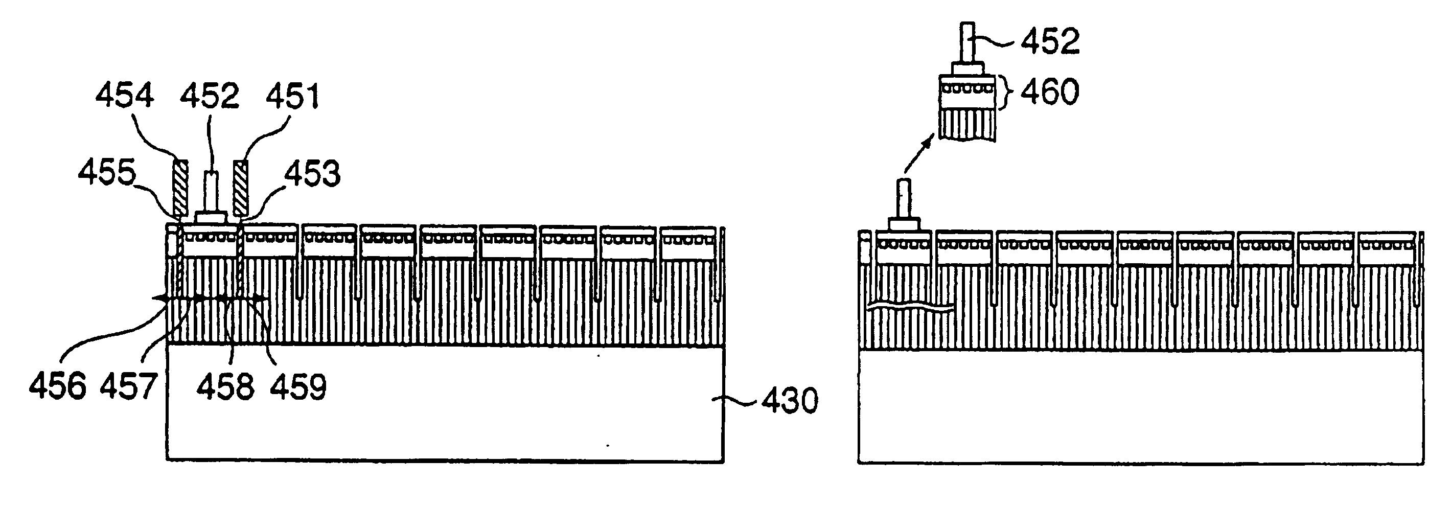
[0092]Next, dicing was performed to form kerfs that partition the substrate into desired regions. The bottom surface of each kerf was located in the ion-implanted layer. After that, when wafer jet was injected from the kerfs, the wafer was separated into a plurality of chips.
[0093]Instead of injecting water jet to the kerfs, a region to be separated into a chip may be locally heated by a laser. Kerfs may be formed bef...
PUM
 Abstract
Description
Claims
Application Information