
Optical wavelength converter

a wavelength converter and optical technology, applied in the field of optical devices, can solve the problems of low conversion efficiency, high power consumption of opto-electronic converters, and high bandwidth limitations of electronic circuitry, and achieve the effects of large non-linear absorption, large non-linear refraction, and high conversion efficiency

Inactive Publication Date: 2005-12-06
CRYSTAL FIBRE AS
View PDF12 Cites 41 Cited by
  • Summary
  • Abstract
  • Description
  • Claims
  • Application Information

AI Technical Summary

Benefits of technology

[0005]An advantage of the invention described in U.S. Pat. No. 5,907,647 is that the signal source and the control source can have the same or different wavelengths, and they can pass through the waveguide in the same or different directions. It is, however, a disadvantage that the devices described by the invention of Eggleton et al. require the inclusion of a long-period waveguide grating. More specifically, it is described by Eggleton et al., how coupling between modes of the waveguide will not take place in the absence of the long-period grating, and, consequently, the switch described by Eggleton will not work, if the grating is omitted.
[0006]In addition to this, it is not described in U.S. Pat. No. 5,907,647, how the long-period grating switches may be used in a wavelength conversion set-up, and it will add complexity to the system to perform the necessary filtering of higher order modes (by the mode separators) discussed in the description by Eggleton. There is, consequently, a need for alternative waveguide components in order to obtain the desired wavelength conversion in optical WDM networks.
[0007]Recently, James S. Shirk and Armand Rosenberg (Laser Focus world, April 2000, pp. 121–129) published results on optical limiters using non-linear photonic crystals fabricated by incorporating organic dyes having a non-linear absorption or refraction. The overall idea behind these components is that the channels of a micro-structured (or nanochannel) glass structure are filled with a non-linear material, whose low-intensity refractive index matches that of glass. When intense light is incident on the structure, the index of the non-linear material is altered, resulting in the development of a bandgap, and that the transmission through the device will eventually drop. As described by Shirk and Rosenberg, recent studies of the optical properties of index-matched phthalocyanine (Pc) dyes have led to the development of materials that combine a large non-linear absorption with large non-linear refraction. Some of these materials have been designed to be liquid or low-melting-point glasses, so that they can be used to fill the tiny open channels in a nanochannel glass crystal. For illumination perpendicular to the nanochannels, as reported in the article by Shirk and Rosenberg, improved limiting properties are observed at short times and for low fluences in the photonic crystal. The reason is that contributions from the non-linear absorption and the photonic bandgap formation combine and add their effects. This is an improvement over the previously described optical limiters using a photonic crystal structure containing a thermal non-linear liquid, such as the one described by Lin et al., Optics Letters, Vol. 23, No. 2, January 1998.
[0008]An additional advantage of the limiter described by Shirk and Rosenberg is that because the decrease in transmission is due, in part, to an increase in reflectivity, the energy load on the non-linear material is reduced, lowering the potential for damage to the material.
[0009]Limiting is observed for 5 ns laser pulses, and the transmitted energy is limited to just over 250 nJ, i.e., the functionality of the device is demonstrated even at modest power density levels.
[0010]The work of Shirk and Rosenberg does not involve optical waveguides, and neither does it describe optical switching using non-linear properties of photonic bandgap structures. Some aspects of optical switching may, however, be found in the paper by Scholz, Hess and Rühle, entitled “Dynamic cross-waveguide optical switching with a non-linear photonic band-gap structure”, published in OPTICS EXPRESS, Vol. 3, No. 1, July 1998. In this paper, a numerical study of a two dimensional all-optical switching device, which consists of two crossed waveguides and a non-linear photonic band-gap structure in the centre. The switching mechanism is based on a dynamic shift of the photonic band edge by means of a strong pump pulse, and it is modelled on the basis of a two dimensional finite volume time domain method. The described method solely considers orthogonal propagation of pump beam and signal beam, and the mentioned waveguiding is limited to two dimensions, i.e., the light is not confined in the third dimension. The work is, however, interesting because it indicates switching times in the order of 10−14 seconds.

Problems solved by technology

For present and future high-speed communication links (operating at bit rates at 10 Gbit / s or more), the power consumption of the opto-electronic converter will be high and bandwidth limitations of electronic circuitry are likely to be encountered.
Coherent converters are transparent to signal format, so many WDM channels may be converted simultaneously, but their conversion efficiency is normally low.
A more serious drawback of the FWM converter is the dependency of the output wavelength on both the pump and the input signal wavelengths, and that two pumps will be needed to ensure polarisation insensitive operation.
It is, however, a disadvantage of the present all-optical converters that they include the use of relatively complex semiconductor optical amplifiers or (as a less studied alternative) long fibre devices for obtaining the desired optical gating properties.
It is, however, a disadvantage that the devices described by the invention of Eggleton et al. require the inclusion of a long-period waveguide grating.
More specifically, it is described by Eggleton et al., how coupling between modes of the waveguide will not take place in the absence of the long-period grating, and, consequently, the switch described by Eggleton will not work, if the grating is omitted.
In addition to this, it is not described in U.S. Pat. No. 5,907,647, how the long-period grating switches may be used in a wavelength conversion set-up, and it will add complexity to the system to perform the necessary filtering of higher order modes (by the mode separators) discussed in the description by Eggleton.
When intense light is incident on the structure, the index of the non-linear material is altered, resulting in the development of a bandgap, and that the transmission through the device will eventually drop.
It is a disadvantage of the switching device described by Scholz, Hess, and Rühle that waveguiding in three dimensions is not described, and that light confinement through optical waveguiding is not utilized.
It is a further disadvantage of the switching device described by Scholz, Hess and Rühle that more than one wavelength is not involved in the switching process.
It is still a further disadvantage of the switching device described by Scholz, Hess and Rühle that the orthogonally propagating pump light and signal light, only has a short interaction length, and therefore requires a very high non-linear response of the material.
It is still a further disadvantage of the switching device described by Scholz, Hess and Rühle that the device works by switching between guidance or reflection of the signal light, and therefore results in a significant reflected signal power.
It is a disadvantage of the optical limiter described by Shirk and Rosenberg that the optical limiters are not applying the property of optical waveguiding.
It is a further disadvantage of the optical limiters described by Shirk and Rosenberg, that they are not making use of the full wavelength span of the non-linear materials, since they fundamentally look at the ability to modify the reflection and transmission properties of a single wavelength through the PBG material.
It is a further disadvantage of the invention described by Eggleton that it does not make use of the improved waveguiding properties of micro-structured optical waveguides, and especially the new properties of photonic bandgap waveguides.

Method used


Image

  • Optical wavelength converter
  • Optical wavelength converter
  • Optical wavelength converter

Examples


Embodiment Construction

[0081]Further scope of applicability of the present invention will become apparent from the detailed description given hereinafter. However, it should be understood that the detailed description and specific examples, while indicating preferred embodiments of the invention, are given by way of illustration only, since various changes and modifications within the spirit and scope of the invention will become apparent to those skilled in the art from this detailed description.

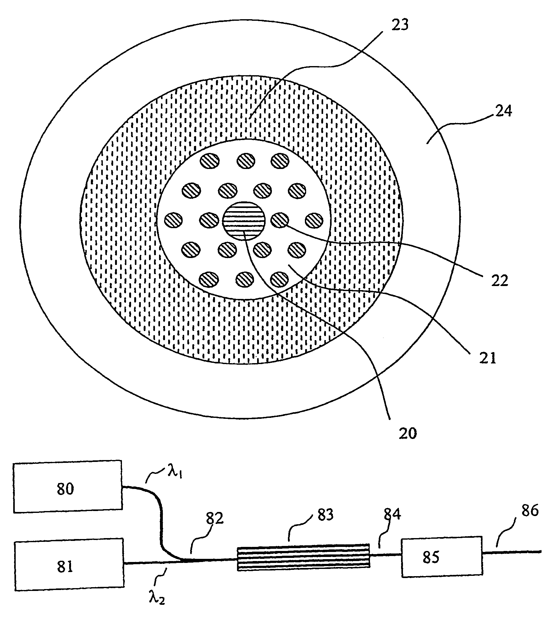
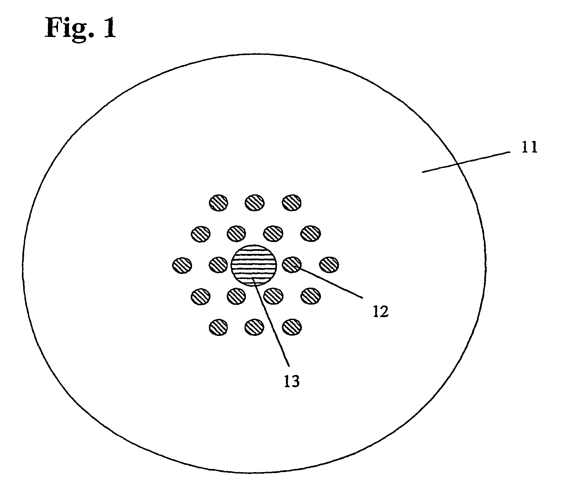
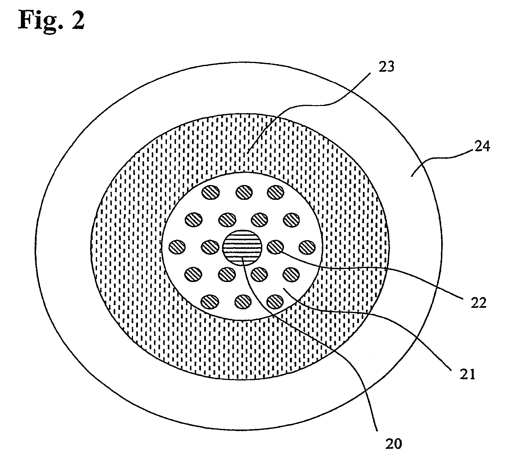
[0082]This description is divided into four parts. Part I describes the fundamental nature and qualitative functionality of the micro-structured non-linear waveguide. Part II describes the qualitative function of an optically controlled switch according to the invention, Part III describes preferred wavelength conversion devices using the optically controlled gating element based on an exemplary micro-structured non-linear waveguide gate, and Part IV describes alternative approaches in the optical control of micr...


PUM

PropertyMeasurementUnit
diameteraaaaaaaaaa
wavelengthsaaaaaaaaaa
index of refractionaaaaaaaaaa

Abstract

An optical wavelength conversion device including a micro-structured optical waveguide, which includes sections with a non-linear material having an index of refraction which changes as a non-linear function of light intensity. The optical waveguide includes a light guiding core region, and is dimensioned for providing spatial overlap between the sections filled with the non-linear material and light propagating within the waveguide. First and second optical light sources may also be included, the second light source having an intensity sufficient to change the refractive index of the non-linear material sufficiently to encode or modulate the light from the first light source through the effect of leaking light from the first light source inside the guiding core to the outside of the guiding core.

Description

FIELD OF INVENTION[0001]The present invention relates to optical devices for conversion of optical signals from one wavelength to another, and in particular such devices realised using micro-structured optical waveguides.BACKGROUND OF THE INVENTION[0002]Wavelength division multiplexing (WDM) is considered one of the most feasible ways to upgrade point-to-point transmission links and to meet the huge demand for transmission capacity in telecommunication systems. As the network technology evolves, it will become important for reconfiguration purposes to be able to perform wavelength conversion or translation within the network or at its interfaces. In order to meet the transmission capacity demands of future optical systems it will be important to make all-optical wavelength converters, and recent research have focussed on various means of providing such functionality (for a review see Stubkjaer et al. IEICE Trans. Electron. Vol. E82-C, No. 2, February 1999). The focus in the research...

Claims


Application Information

Patent Timeline
Patent Type & Authority Patents(United States)
IPC IPC(8): G02B6/02G02B6/036G02B6/122G02F1/35G02F1/365
CPCB82Y20/00G02B6/02G02B6/02338G02B6/02347G02B6/02357G02B6/0238G02B6/03627G02B6/1225G02F1/3515G02F1/365G02F2201/02G02F2202/32
Inventor BJARKLEV, ANDERSBROENG, JESLIBORI, STIG EIGIL BARKOU
Owner CRYSTAL FIBRE AS
Learn More