Buffer/driver circuits

a buffer/driver circuit and circuit technology, applied in logic circuits, pulse techniques, reliability increasing modifications, etc., can solve the problems of not achieving an adequate reduction of leakage power dissipation, affecting the production efficiency of small devices, and a significant portion of power dissipation, so as to reduce the high leakage current and reduce the leakage. the effect of low leakag

Inactive Publication Date: 2005-12-13
IBM CORP
View PDF4 Cites 8 Cited by
  • Summary
  • Abstract
  • Description
  • Claims
  • Application Information

AI Technical Summary

Benefits of technology

[0014]A buffer / driver topology for interfacing power-gated and non power-gated circuitry employs three parallel circuit paths. One path comprises two small area inverters in series between the buffer / driver input and output. A first parallel path has a first input coupled to the buffer / driver input and a first output coupled to the buffer / driver output. The first parallel path comprises a first inverter with power-gating applied to the negative power supply voltage. The output of the first inverter is coupled to a PFET which is a large device used to provide current for pulling the buffer / driver output quickly to the positive power supply voltage level. The source of the PFET is coupled to the positive power supply voltage and the drain of the PFET is coupled to the buffer / driver output. Likewise, the second parallel path comprises a second inverter with power-gating applied to the positive power supply voltage. The output of the second inverter is coupled to an NFET which is a large device used to provide current for pulling the buffer / driver output quickly to the negative power supply voltage level. The source of the NFET is coupled to ground and the drain of the NFET is coupled to the buffer / driver output. When the first and second inverters are power-gated, the two small area inverters maintain the logic state of the buffer / driver output. Since the devices in the small area inverters are small devices, they may be configured to have low leakage. The large NFET and PFET coupled to the output have their gates “floated” when the first and second inverters are power-gated, thus reducing the high leakage current of these devices. Additional configurations allow circuitry where only the pull down or pull up devices are large and employ power-gating. The non power-gated level is set by the first and second inverter string. Other embodiments utilize more than two inverting stages in series wherein the first stage may be multi-input inverting logic stage.

Problems solved by technology

As CMOS circuits become smaller, leakage current that results when voltage is applied to the gate of the field effect transistors becomes a significant portion of the power dissipation.
Leakage power may become the limiting factor in how small devices may be manufactured.
However, this may not achieve an adequate reduction in leakage power dissipation.
Interfacing between circuits in a power-gated domain and circuits in a non-power-gated domain may prove difficult.
While the benefits of power-gating are known, there is no consensus on strategies to preserve logic states of outputs in the power-gated domains.
Therefore, one would expect the large devices to exhibit large gate-leakage current when the technology has gate oxides that are very thin.
Likewise, logic regions with a high number of logic gates may exhibit a large gate-leakage current due to the large number of devices that are in strong inversion at any one static time (between clock transitions).
Typically a power gating is applied to a block of circuits which makes it difficult to provide timing control of the power gating.

Method used


Image

  • Buffer/driver circuits
  • Buffer/driver circuits
  • Buffer/driver circuits

Examples


Embodiment Construction

[0026]In the following description, numerous specific details are set forth to provide a thorough understanding of the present invention. However, it will be obvious to those skilled in the art that the present invention may be practiced without such specific details. In other instances, well-known circuits may be shown in block diagram form in order not to obscure the present invention in unnecessary detail. For the most part, details concerning timing, and the like have been omitted inasmuch as such details are not necessary to obtain a complete understanding of the present invention and are within the skills of persons of ordinary skill in the relevant art.

[0027]Refer now to the drawings wherein depicted elements are not necessarily shown to scale and wherein like or similar elements are designated by the same reference numeral through the several views.

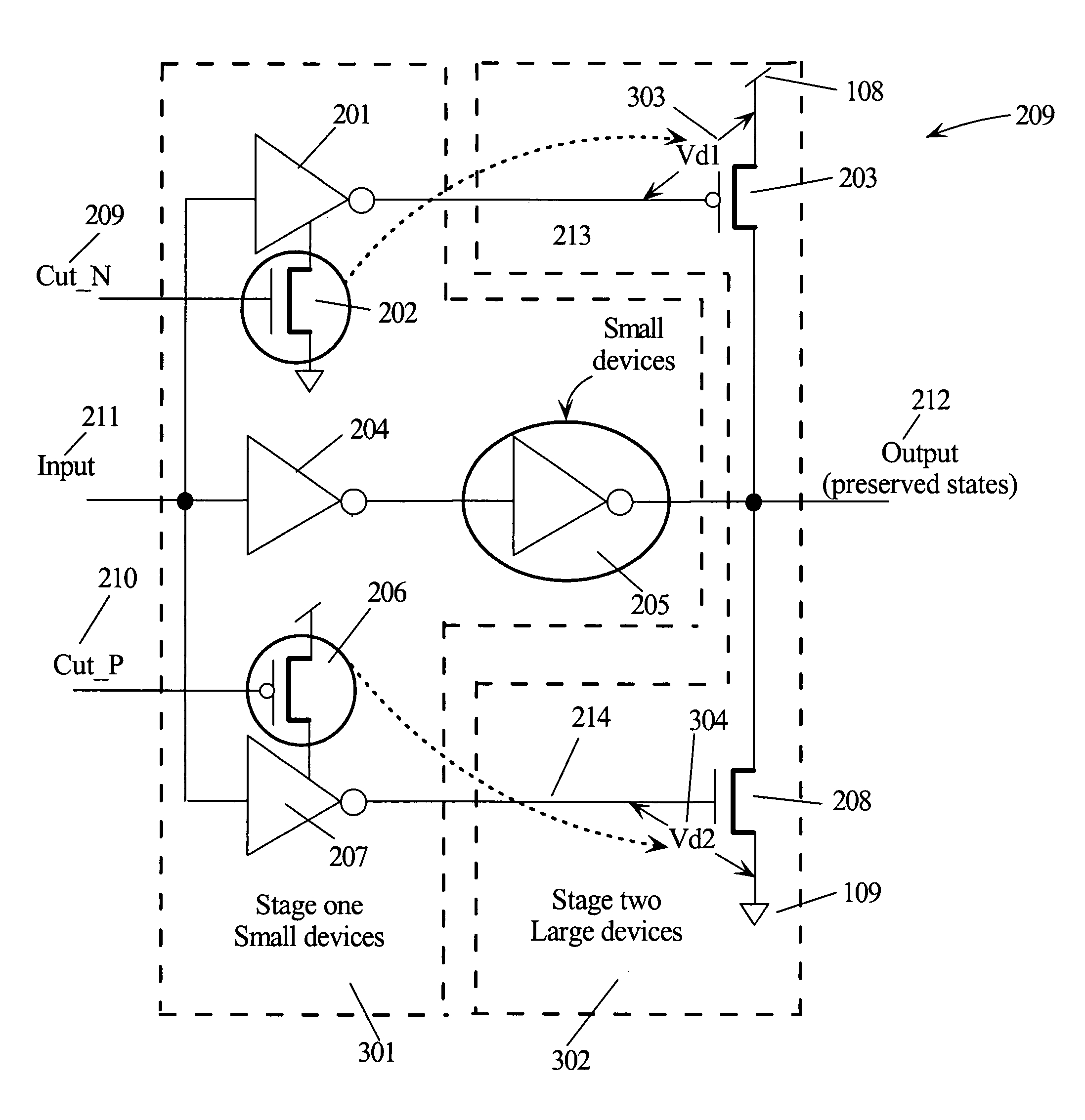
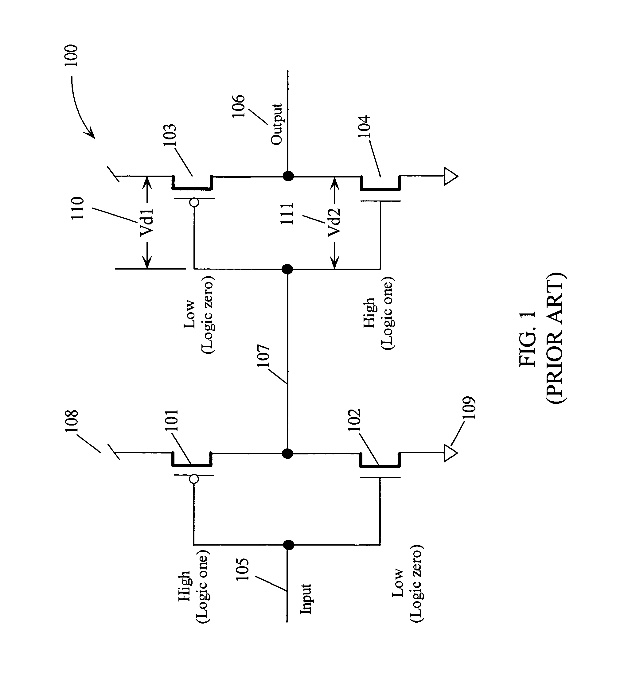
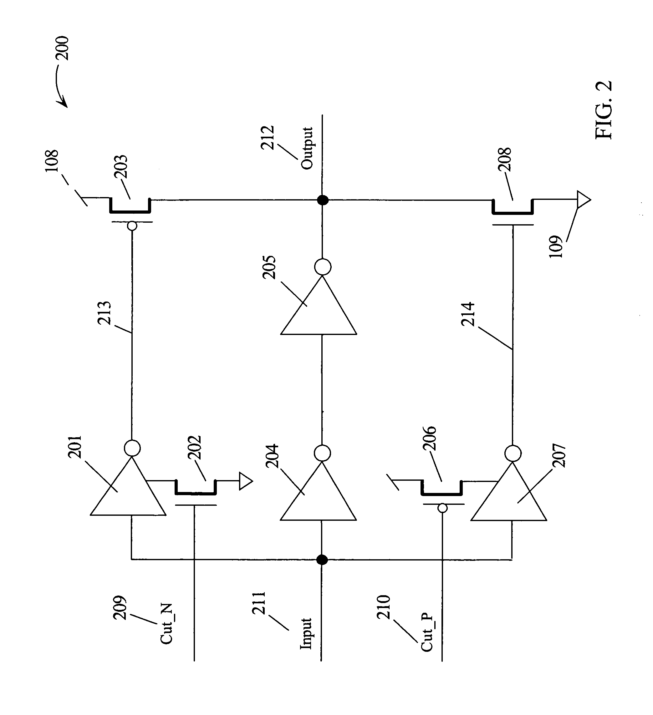
[0028]FIG. 1 is a circuit diagram of a prior art non-inverting buffer 100 comprising two inverting stages. Buffer 100 is coupled...


PUM


Abstract

A buffer / driver having large output devices for driving multiple loads is configured with three parallel paths. The first logic path is made of small devices and is configured to provide the logic function of the buffer / driver without the ability to drive large loads. Second and third logic paths have the logic function of the first logic path up to the last inverting stage. The last inverting stage in each path is a single device for driving the logic states of the buffer output. The second and third logic paths have power-gating that allows the input to the pull-up and pull-down devices to float removing gate-leakage voltage stress. When the second and third logic paths are power-gated, the first logic path provides a keeper function to hold the logic state of the buffer output. The buffer / driver may be an inverter, non-inverter, or provide a multiple input logic function.

Description

GOVERNMENT RIGHTS[0001]This invention was made with Government support under NBCH30390004 awarded by DEFENSE ADVANCED RESEARCH PROJECT AGENCY. The Government has certain rights in this invention.TECHNICAL FIELD[0002]The present invention relates in general to complementary metal oxide semiconductor (CMOS) circuits and, in particular, to circuit methodologies for reducing leakage in sub-100 nm technologies.BACKGROUND INFORMATION[0003]Oxide tunneling current in metal oxide silicon (MOS) field effect transistors (FET) is a non-negligible component of power consumption as gate oxides get thinner, and may in the future become the dominant leakage mechanism in sub-100 nm complementary MOS (CMOS) circuits. The gate current is dependent on various conditions and three main static regions of operation may be identified for a MOSFET. The amount of gate-leakage current differs by several orders of magnitude from one region to another. Whether a transistor leaks significantly or not is also aff...

Claims


Application Information

Patent Timeline
Patent Type & Authority Patents(United States)
IPC IPC(8): H03K17/16H03K19/00H03K19/003H03K19/017
CPCH03K19/0016H03K19/00361H03K19/01721
Inventor KUANG, JENTE B.NGO, HUNG C.NOWKA, KEVIN J.
Owner IBM CORP
Why Eureka
Try Eureka