Semiconductor integrated circuit

a technology of integrated circuits and semiconductors, applied in the field of semiconductor integrated circuits, can solve the problems of slow conversion process speed and inability to decrease achieve the effects of accelerating the process time for a/d conversion, and reducing the impedance of ladder-type resistors

a technology of integrated circuits and semiconductors, applied in the field of semiconductor integrated circuits, can solve the problems of slow conversion process speed and inability to decrease achieve the effects of accelerating the process time for a/d conversion, and reducing the impedance of ladder-type resistors

US6975262B2Inactive Publication Date: 2005-12-13RENESAS TECH CORP

Image

  • Semiconductor integrated circuit
  • Semiconductor integrated circuit
  • Semiconductor integrated circuit

Examples


Embodiment Construction

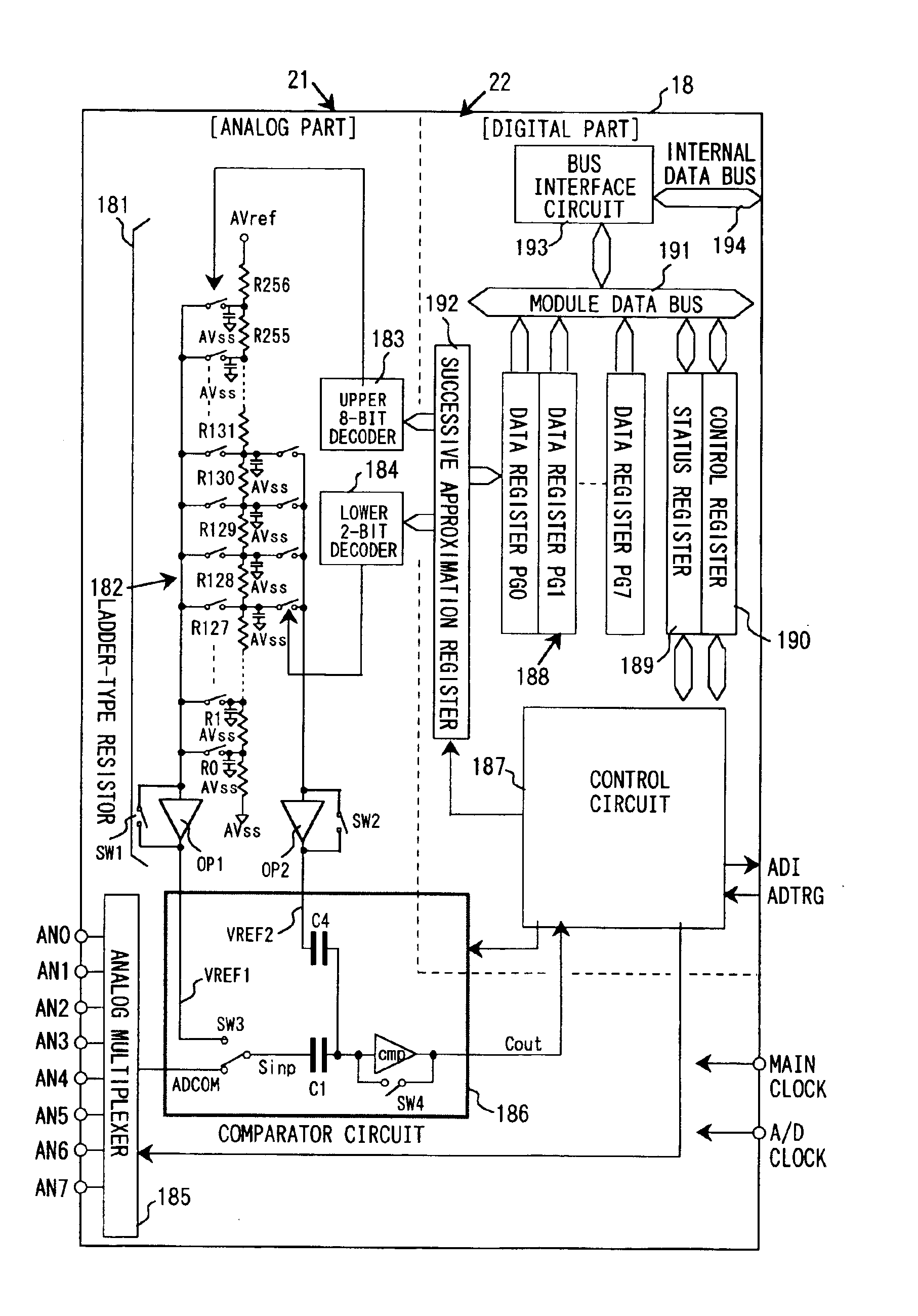
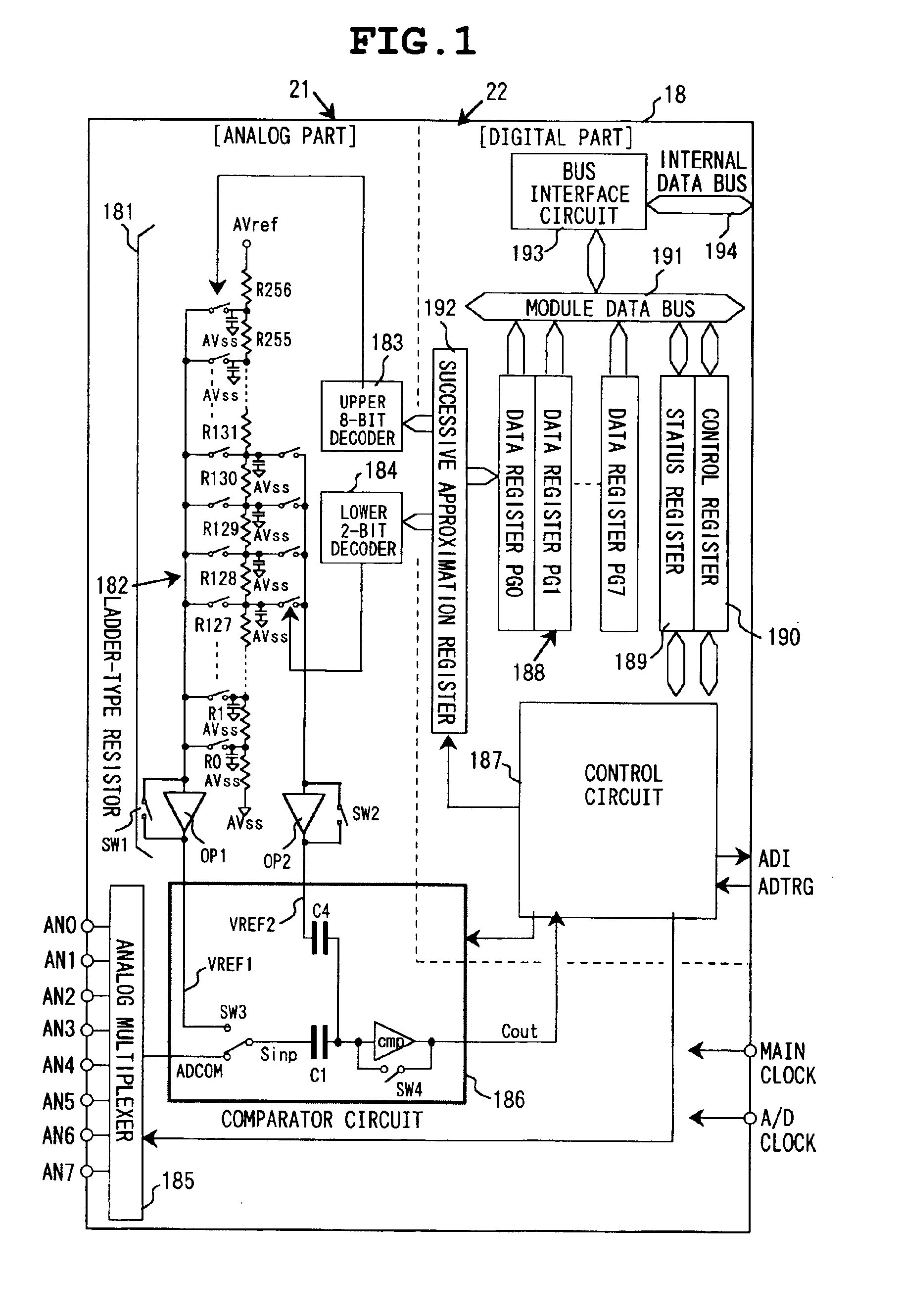
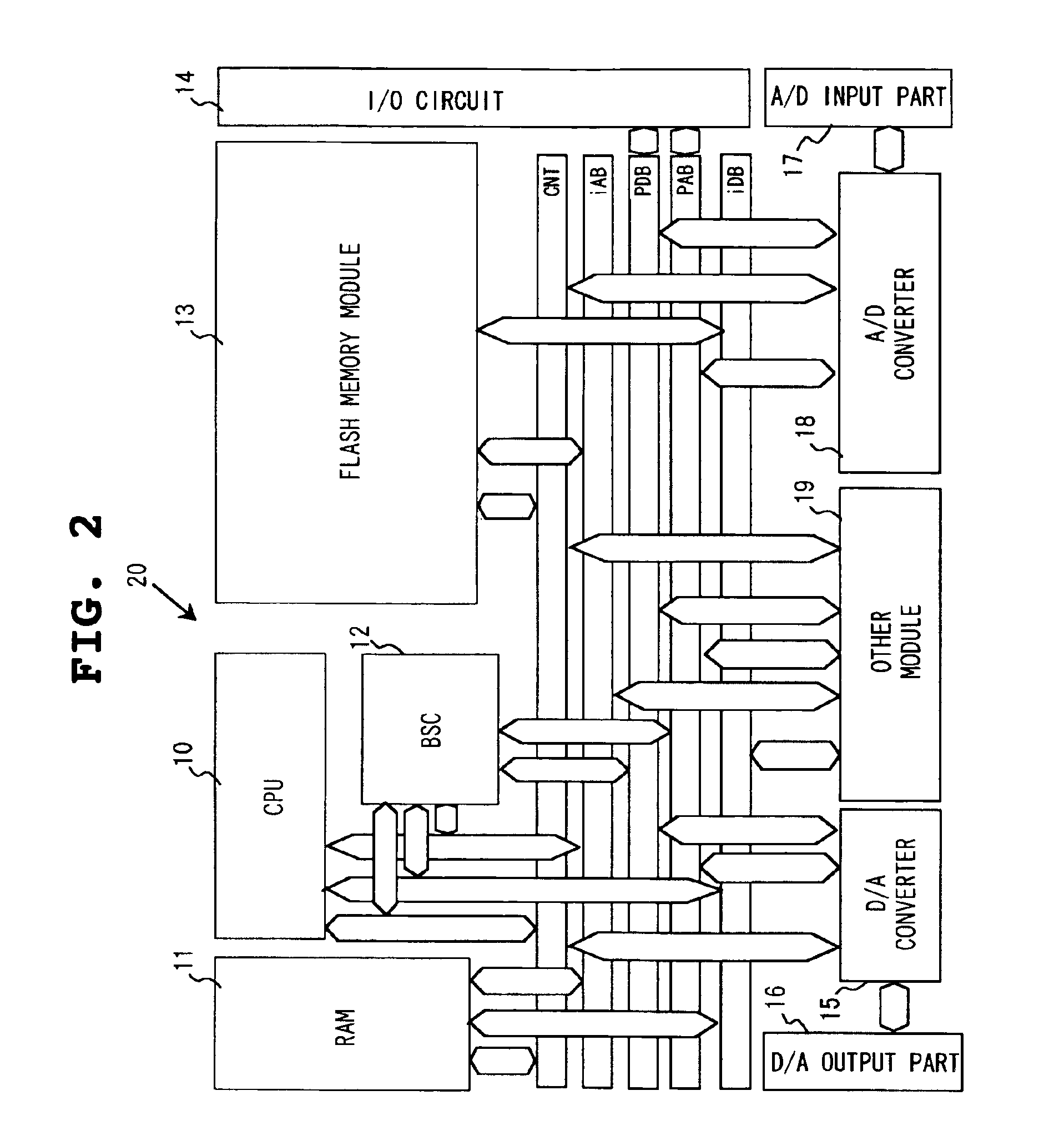
[0041]Referring to FIG. 2, there is shown an example of the configuration of a microcomputer as an example of a semiconductor integrated circuit according to the invention. While the microcomputer 20 shown in FIG. 2 is not particularly limited, the microcomputer 20 includes: a CPU (Central Processing Unit) 10 for carrying out a given operation process according to a program control method; a RAM (Random Access Memory) 11 for providing a work area for the CPU 10 and temporarily storing the data resulting from the execution of a program, etc.; a BSC (Bus State Controller) 12 for bus state control, such as weight insertion; a flash memory module 13 for storing the program the CPU 10 executes and fixed data required for control; an I / O circuit (input-output circuit) 14 for enabling various signals to be input from and output to the outside; a D / A converter 15 for converting a digital signal into an analog signal; a D / A output part 16 capable of outputting an analog signal produced in th...


PUM


Abstract

A semiconductor integrated circuit including an A / D converter capable of converting an analog signal accepted through an external terminal into a digital signal. The A / D converter includes: a ladder-type resistor for generating a reference voltage; a set of first operational amplifiers, each accepts an output voltage of the ladder-type resistor; a set of first switches, each capable of short-circuiting an input terminal and an output terminal of corresponding one of the first operational amplifiers thereby to allow an offset correction of the corresponding first operational amplifier to be made; and a comparator circuit for comparing an output voltage of each of the first operational amplifiers with the analog signal. The A / D converter can reduce a current output from the ladder-type resistor and speed up charge and discharge of the sampling capacitor.

Description

CLAIM OF PRIORITY[0001]The present application claims priority from Japanese application JP 2003-187566 filed on Jun. 30, 2003, the content of which is hereby incorporated by reference into this application.BACKGROUND OF THE INVENTION[0002]The present invention relates to a semiconductor integrated circuit, and a technique intended to increase conversion speeds of A / D (analog-to-digital) converter and D / A (digital-to-analog) converter and shorten the conversion times thereof, for example, a technique useful in applications to microcomputers.[0003]In a semiconductor integrated circuit including an A / D converter and D / A converter, especially in a microcomputer, an analog signal entered from the outside is converted into a digital signal in the A / D-converter and then supplied to the CPU (central processing unit). In addition, the result of an operation process in the CPU may be converted into an analog signal by the D / A converter to output. Regarding such A / D converter, as a technique ...

Claims


Application Information

Patent Timeline
13 Dec 2005
Publication
US6975262B2
IPC
G11C7/00; H03M1/14; G11C7/16; H03M1/10; H03M1/46; H03M1/68; H03M1/76
CPC
H03M1/1023; H03M1/46; H03M1/682; H03M1/765; G11C7/16; G11C7/00
Inventors
YADA, NAOKI; SAITO, YASUYUKI