Solid-state imaging device with the elimination of thermal noise

a solid-state imaging and thermal noise technology, applied in the direction of radioation control devices, television system scanning details, television systems, etc., can solve the problems of thermal noise picture quality deterioration, etc., and achieve the effect of reducing the effect of thermal nois

Inactive Publication Date: 2005-12-13
FUJITSU LTD
View PDF7 Cites 56 Cited by
  • Summary
  • Abstract
  • Description
  • Claims
  • Application Information

AI Technical Summary

Benefits of technology

[0021]According to the above-mentioned second aspect, it is possible to reduce the effects of thermal noise by making use of a differential voltage between a reset level on which a thermal noise is superimposed, and a detection level added thereto. Further, because...

Problems solved by technology

However, a conventional APS of the above constitution has a charge storage capacitor and a source follower or other such amplifier, a fixed pattern noise (FPN) in generated.
It results in picture quality deterioration.
However, with this method, there remains the problem that the reset noise (kTC noise) before storing a quantity-of-light signal and the reset noise after reading the signal are added so as to increase the random noise level, and the S/N ratio deteriorates compared to that of a CCD solid-state imaging device.
However, since this kTC noise has random fluctuations with time as hereinabove, the kTC noise that is superimposed on the initial reset level differs from the kTC noise that is superimposed on the second reset level, making it impossible to curb kTC noise even by using the difference between these two levels to curb fixed pattern noise (variations in threshold voltage VT).
However, for the conventional example of FIG. 8, firstly, the problem is that because there is a buffer B1, which is a source follower, it is not possible to remove the...

Method used


Image

  • Solid-state imaging device with the elimination of thermal noise
  • Solid-state imaging device with the elimination of thermal noise
  • Solid-state imaging device with the elimination of thermal noise

Examples


first embodiment

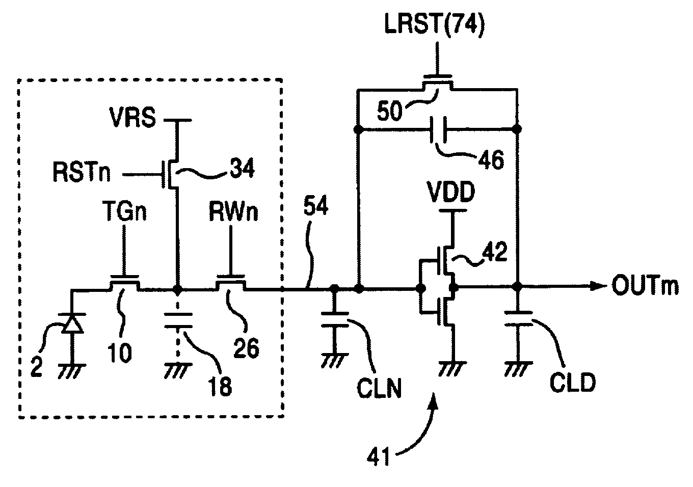
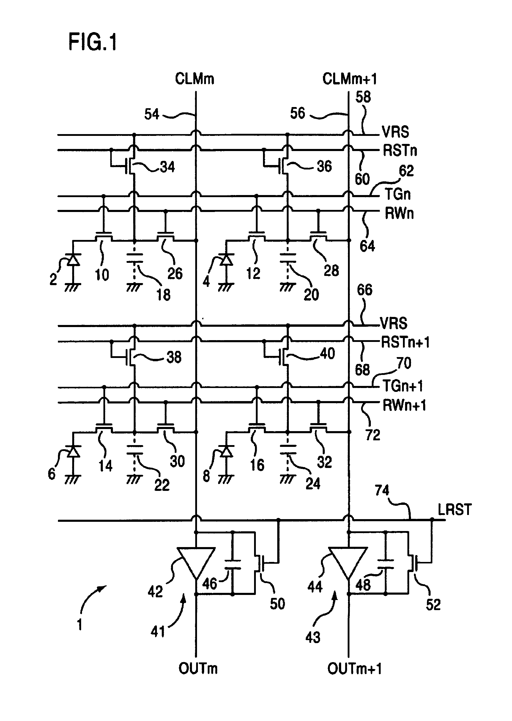
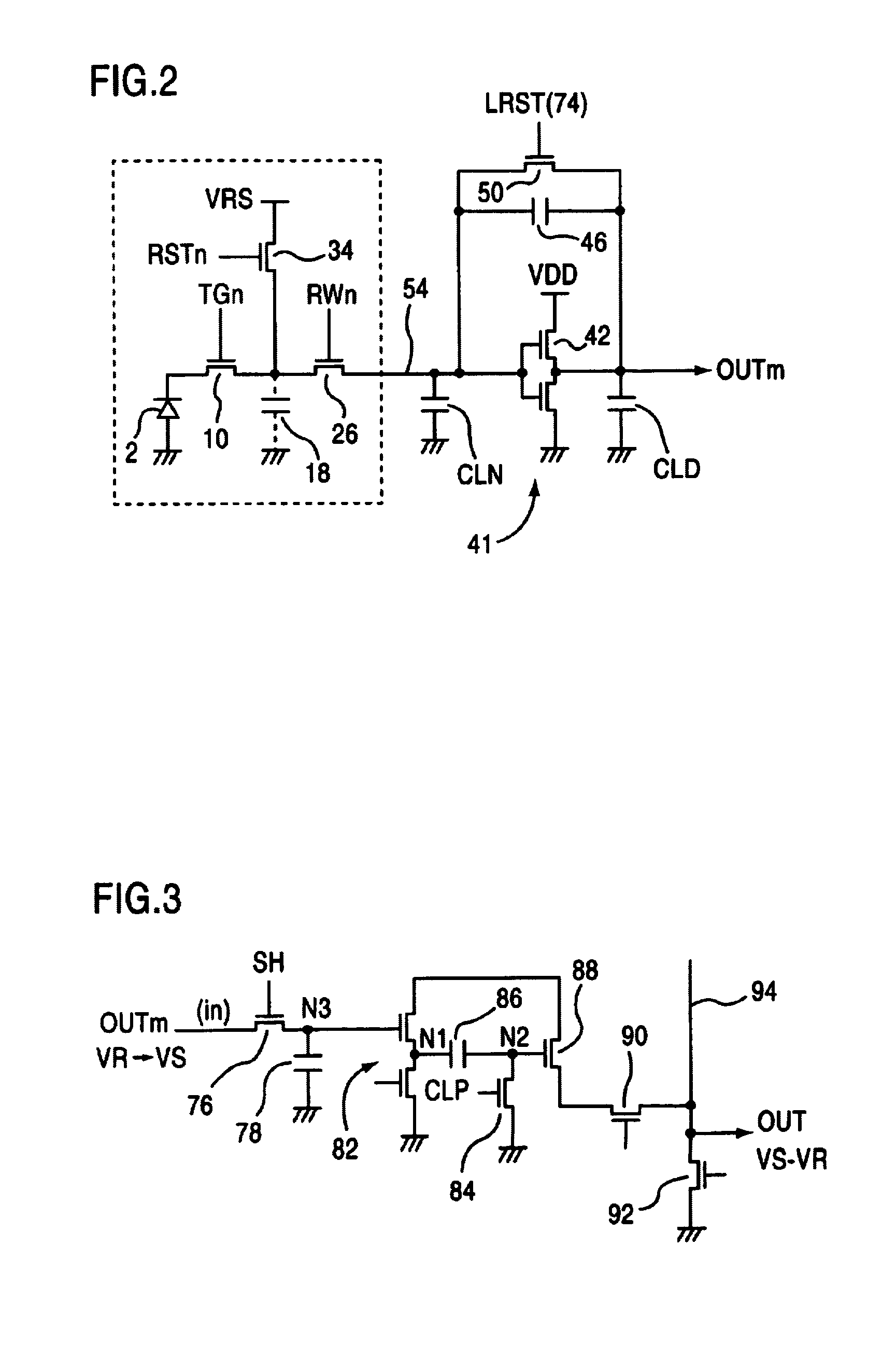
[0036]A solid-state imaging device according to the present invention will be explained by using FIG. 1 through FIG. 6. First, a simplified constitution of a solid-state imaging device according to the embodiment will be explained using FIG. 1.

[0037]FIG. 1 shows a circuit example of an XY address-type image sensor 1 corresponding to 2×2 pixels in a solid-state imaging device of the embodiment. MOSFET transfer gates (TG) 10, 12, 14, 16 are connected, respectively, to the cathode sides of photodiodes 2, 4, 6, 8 of the light-sensitive portions of each pixel. Furthermore, photodiode 2 in the light-sensitive portion can be constituted from a photogate. Source junction capacitors of the floating diffusion (FD) region of between transfer gates 10, 12, 14, 16 and MOSFET horizontal selection switches 26, 28, 30, 32 are used as detection capacitors 18, 20, 22, 24. The gate electrodes of transfer gates 10, 12 are connected to transfer gate control line 62, and the gate electrodes of transfer g...

second embodiment

[0082]As a characteristic of the second embodiment, there provides a reset gate 11 for removing a charge stored in the well of photodiode 2. Moreover, when this reset gate 11 is ON, the electron well of photodiode 2 is completely depleted, and is reset to an absolute level determined by the doping concentration and depth of low-concentration n region 113. Therefore, thermal noise is not contained therein. And by controlling the timing at which reset pulse Rn is applied, it is possible to achieve either an electron shutter function, or a exposure control function.

[0083]FIG. 12 is a diagram showing a variation of the second embodiment. As shown in the cross-sectional view of FIG. 12A, the P-type well region 111 of the central portion is formed deeply, and a low-concentration n region 113, which forms a photodiode 2, is formed therein. Therefore, there is no blooming suppressing function that uses a shallow P-type well region 111A as shown in FIG. 10A. In place thereof, in the example ...


PUM


Abstract

A solid-state imaging device comprises: a plurality of pixels including a light-sensitive portion (2) for photoelectrically converting incident light, a transfer gate (10) for transferring a charge stored in the light-sensitive portion, a resettable detection capacitor (18) for storing the charge transferred from the transfer gate, and a selection switch (26) for outputting a charge of the detection capacitor according to a selection signal RWn; a charge amplifier (41) for converting the detection capacitor charge, which is outputted from the pixels, to a voltage; and a correlated double sampling circuit (86) for obtaining a voltage difference between a reset level and a detected level converted by the charge amplifier. According to the above device, a thermal noise is eliminated due to the correlated double sampling circuit. Further, a fixed pattern noise is not generated due to the pixel circuit structure.

Description

BACKGROUND OF THE INVENTION[0001]1. Field of the Invention[0002]The present invention relates to a solid-state imaging device constituted by a semiconductor device, and more particularly to an XY address-type solid-state imaging device manufactured by a CMOS process. In addition, the present invention relates to a solid-state imaging device capable of eliminating the effects of fixed pattern noise and thermal noise.[0003]2. Description of the Related Art[0004]Solid-state imaging devices include XY address-type solid-state imaging devices in which an image sensor is formed by CMOS, and the so-called CCD solid-state imaging devices constituting a charge transfer-type image sensor. Because the XY address-type solid-state imaging device, which utilizes a CMOS image sensor, does not require a special manufacturing process, and is driven by a single power source with smaller power consumption, and furthermore, is capable of mounting various signal processing circuits on the same chip, it ...

Claims


Application Information

Patent Timeline
IPC IPC(8): H01L31/10H01L27/146H04N5/335H04N5/363H04N5/365H04N5/374H04N5/3745H04N5/378
CPCH04N5/3575H04N5/37452H04N25/616H04N25/771
Inventor MIYAMOTO, YOSHIHIRO
Owner FUJITSU LTD
Why Eureka
Try Eureka