

Film quality inspecting method and film quality inspecting apparatus
a film quality inspection and film inspection technology, applied in the direction of instruments, optics, material analysis, etc., can solve the problems of deteriorating the yield of manufacturing tft, inability to obtain information of re-crystallization after actual poly-crystallization, and method cannot be applied to a field production lin
- Summary
- Abstract
- Description
- Claims
- Application Information
AI Technical Summary
Benefits of technology
Problems solved by technology
Method used
Image

Examples
second embodiment
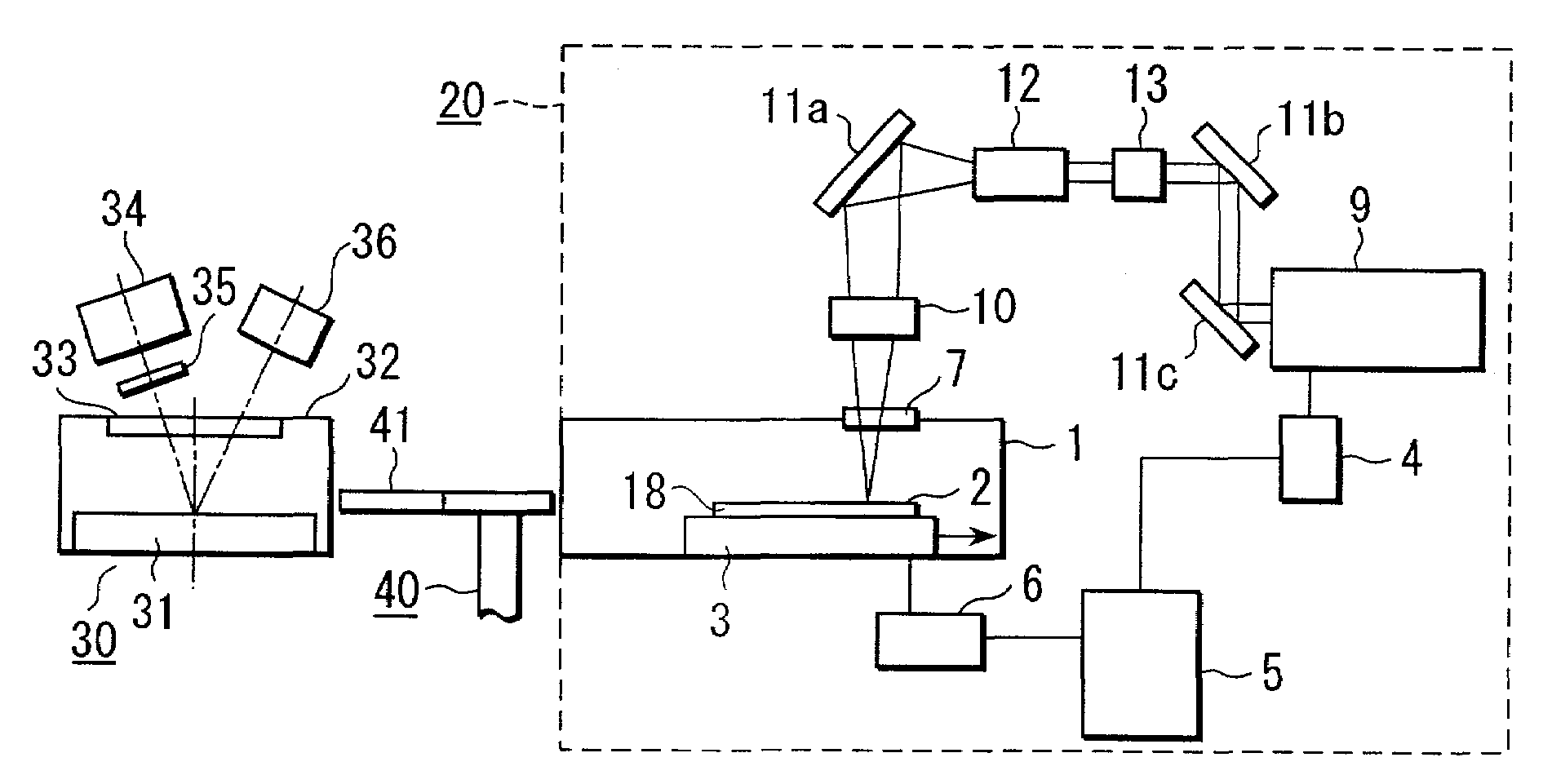
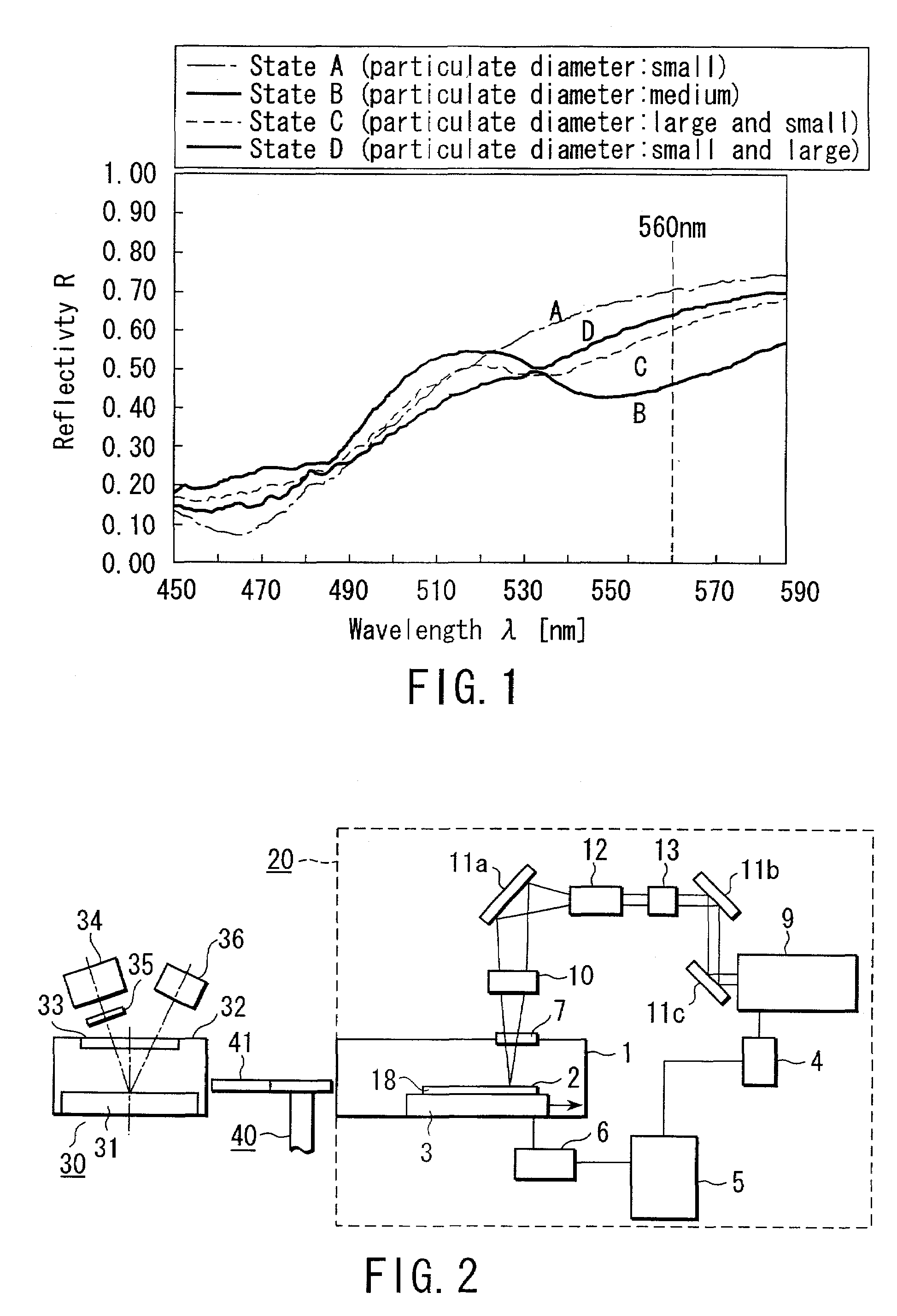
[0078]FIGS. 4–10 show the present invention.
first embodiment
[0079]As mentioned above with the first embodiment, by the low-temperature p-Si can be manufactured by a low temperature process by utilizing excimer laser annealing processing. It is thus possible to commercially produce a TFT-LCD made of p-Si using a large glass substrate having almost the same size as that by a-Si.
[0080]By using p-Si, the TFT can be small sized and a driver IC can be incorporated, to solve the problems such as deterioration in numerical aperture, restrictions on higher definition, etc., thus giving such features suitable for a mobile LCD as higher brightness, lower power dissipation, higher definition, improved durability, lighter weight, smaller thickness, etc.
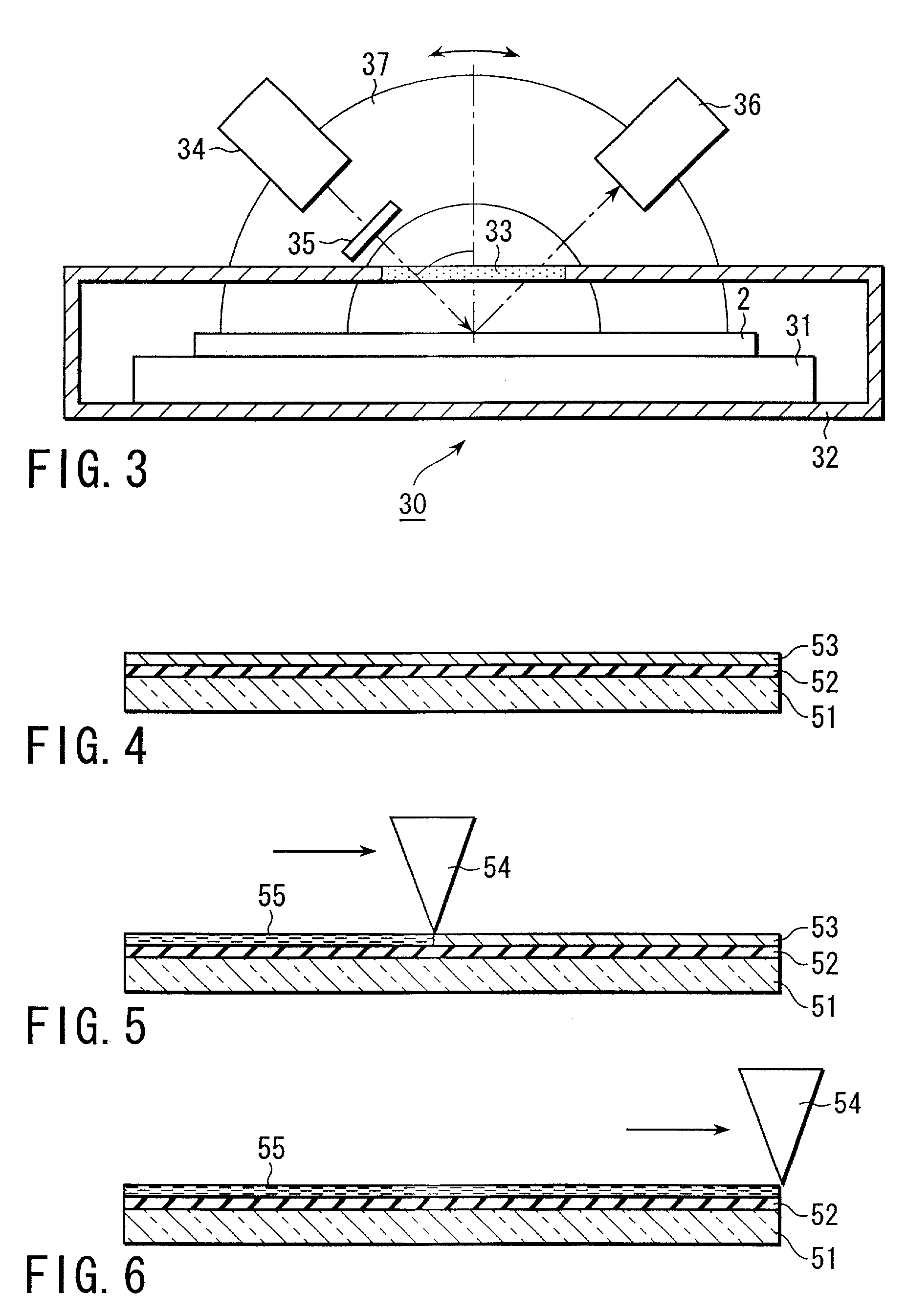
[0081]As is clear from the schematic diagrams shown in FIGS. 4–6, to manufacture on a TFT in which a p-Si film is formed on a glass substrate 51, it is necessary to form the p-Si film on the glass substrate 51 without deforming the glass substrate 51. To form the p-Si film under such restrictions, as shown...
PUM
 Abstract
Description
Claims
Application Information