Direct writing of optical devices in silica-based glass using femtosecond pulse lasers

a technology of optical devices and pulse lasers, which is applied in the direction of photomechanical equipment, instruments, manufacturing tools, etc., can solve the problems of detracting from the waveguide properties of glass, increasing pulse energy, and physical damage to glass, so as to maximize the writing rate, maximize the exposure intensity, and increase the repetition rate preferably

Inactive Publication Date: 2005-12-20
CORNING INC
View PDF30 Cites 23 Cited by
  • Summary
  • Abstract
  • Description
  • Claims
  • Application Information

AI Technical Summary

Benefits of technology

[0011]Our invention in one or more of its embodiments provides improved direct-write methods of forming light-guiding and light-managing structures within silica-based material substrates. Three-dimensional light-guiding and light-managing structures, such as waveguides and gratings, are direct-written into bulk glass at efficient rates using pulse energy levels limited for achieving desired changes in refractive index while avoiding other changes harmful to waveguiding properties of the bulk glass.
[0018]In accordance with another aspect of the invention, it has been discovered that soft silica-based materials exhibit increased sensitivity to ultra-fast laser writing of optical structures in the bulk glass. Femtosecond laser-induced refractive index changes can be more easily produced in silica-based compositions having an annealing point that is lower than that of the 5 mol. % germania (GeO2)-95 mol. % silica (SiO2) system in that lower pulse energies and faster translation speeds can produce equivalent increases in refractive index as harder silica-based materials.
[0019]In accordance with another aspect of the invention, a method is provided to directly write light-guiding structures in glass using short-pulse lasers with substantially no physical damage of the glass.

Problems solved by technology

However, the substantial increases in pulse energy beyond the saturation point are accompanied by physical damage to the glass.
However, at pulse energies well above 1 microjoule (μJ) in the same writing configuration, physical damage occurs that detracts from the waveguiding properties of the glass.
Small voids or other discontinuities are believed to be formed in the bulk glass, which disrupt the transmission of light.

Method used


Image

  • Direct writing of optical devices in silica-based glass using femtosecond pulse lasers
  • Direct writing of optical devices in silica-based glass using femtosecond pulse lasers
  • Direct writing of optical devices in silica-based glass using femtosecond pulse lasers

Examples


example 1

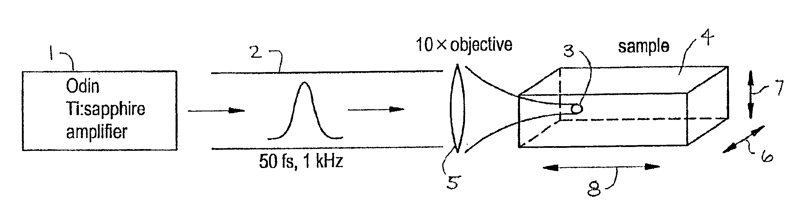
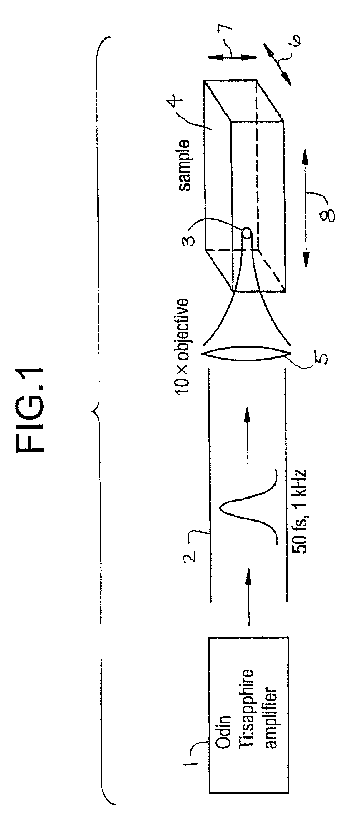
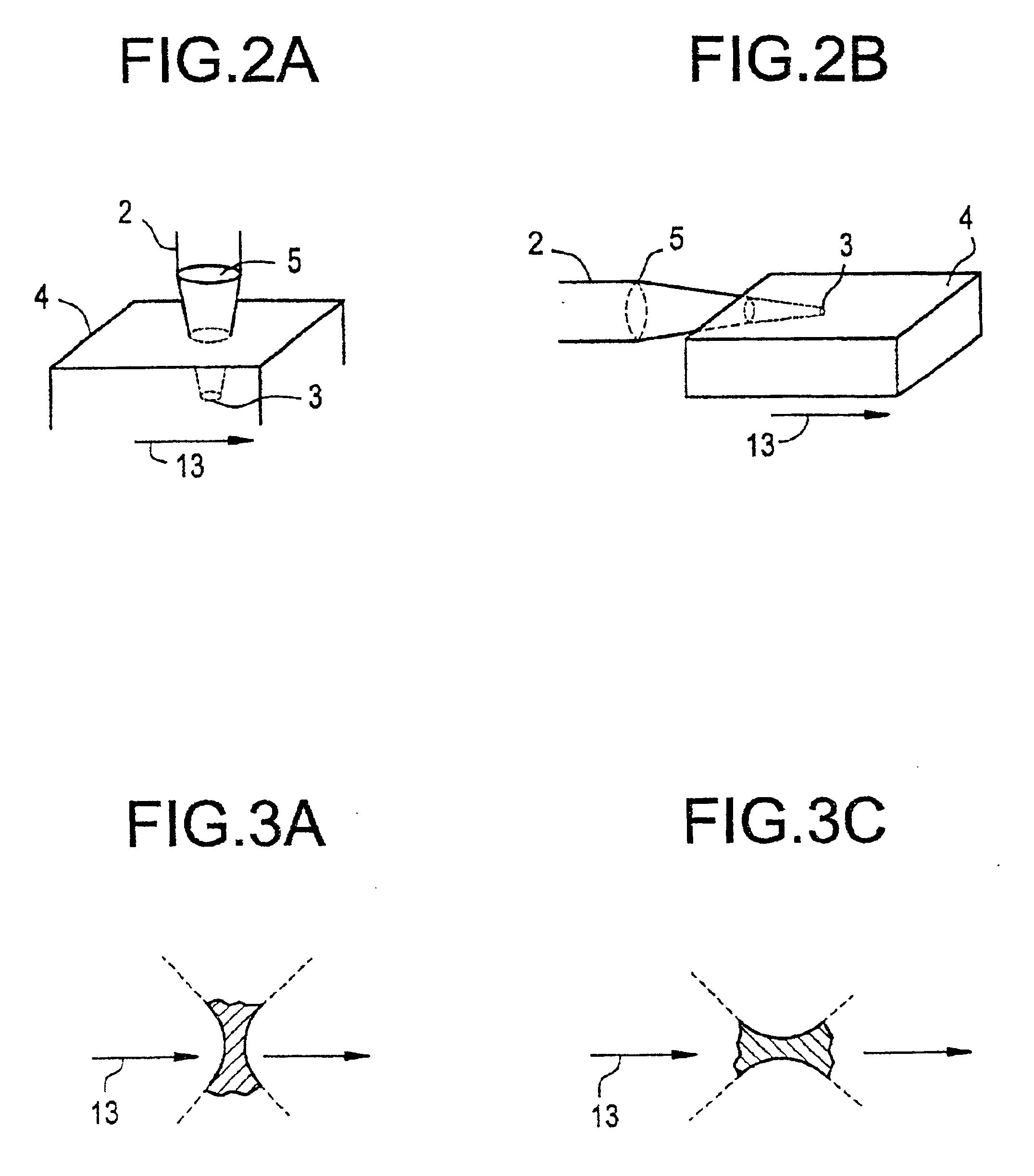
[0066]Pulses from a Ti:Sapphire multi-pass amplifier which were 60-fs in duration and had pulse energies of approximately 1 μJ were focused with a 10× (0.16 NA) microscope objective into fused-silica glass samples mounted on a computer-controlled high-precision 3-D translation stage. The fused-silica samples were translated through the focal point of the beam at a rate of 30 μm / s. Waveguide structures were created within the bulk material.

example 2

[0067]A 830 nm laser was used to deliver 40 fs pulses at a 1 kHz repetition rate. The energy per pulse was from about 1 μJ to about 5 μJ. The beam was focused into the glass below the surface with a lens having a numerical aperture of 0.16 in air. The sample was moved under the beam at a rate of about 5 μm / s to about 100 μm / s. The experimental conditions were kept constant for exposure to samples of fused silica and for 14 wt. % GeO2-86 wt. % SiO2. The beam was focused about 1 mm below the surface of the glass. For samples irradiated at the same exposure conditions, the diameter of the laser-affected region of the germania-silica sample was about twice that of the fused-silica sample. From this result, we concluded that the germania-silica material was more sensitive to refractive index changes induced by ultra-fast laser exposure than fused silica.

example 3

[0068]Substrates of various glass compositions, i.e., SiO2 (Corning product 7980), 22 wt. % GeO2-78 wt. % SiO2, and 9 wt. % B2O3-91 wt. % SiO2, were exposed to focused laser radiation by the axial-write method. The laser wavelength was 830 nm. The pulse duration was 40 fs. The energy per pulse was 1.0 μJ. The repetition rate was 1 kHz. The scan speed was 20 μm / s. After exposure, the induced refractive index change at 633 nm was estimated from the far-field pattern of the waveguide produced. The induced refractive index change results are tabulated below in Table 1. The annealing point of each of these materials is also reported in Table 1.

[0069]

TABLE 1Induced refraction index change (Example 3)Glass Composition(% based onAnnealing PointInduced Refractiveweight)(° K)Index ChangeSiO2 (Corning 7980)1261-13230.000378% SiO2 - 22% GeO213110.000991% SiO2 - 9% B2O310730.0030


PUM

PropertyMeasurementUnit
wavelengthaaaaaaaaaa
absorption edgeaaaaaaaaaa
poweraaaaaaaaaa

Abstract

The invention relates to methods of writing a light-guiding structure in a bulk glass substrate. The bulk glass substrate is preferably made from a soft silica-based material having an annealing point less than about 1380° K. A pulsed laser beam is focused within the substrate while the focus is translated relative to the substrate along a scan path at a scan speed effective to induce an increase in the refractive index of the material along the scan path. Substantially no laser-induced physical damage of the material is incurred along the scan path. Various optical devices can be made using this method.

Description

RELATED APPLICATIONS[0001]This application is a continuation-in-part of U.S. patent application Ser. No. 09 / 627,868, filed Jul. 28, 2000, now abandoned, which claims priority to U.S. Provisional Patent Application No. 60 / 146,274, filed Jul. 29, 1999, entitled Direct Writing of Optical Devices in Silica-Based Glass Using Femtosecond Pulse Lasers of Nicholas F. Borrelli and Charlene Smith and to U.S. Provisional Patent Application No. 60 / 172,122, filed Dec. 17, 1999, entitled Femtosecond Laser Writing of Glass, Including Borosilicate, Sulfide and Lead Glasses of Nicholas F. Borrelli, David L. Morse, Alexander Streltsov, and Bruce Aitken.TECHNICAL FIELD[0002]The invention relates to methods for efficiently forming optical devices in glass. Specifically, the invention relates to direct-write methods of forming light-guiding structures in glass compositions through light-induced refractive index changes using pulsed lasers having a pulse duration less than about 150 femtoseconds (fs). Th...

Claims


Application Information

Patent Timeline
Patent Type & Authority Patents(United States)
IPC IPC(8): B23K26/00B23K26/06C03C23/00G02B6/12G02B6/13G02B6/132G11C13/04
CPCB23K26/0635C03C23/0025G02B6/13G02B6/132G11C13/04G11C13/041G02B2006/12107G02B2006/12147G02B2006/12171Y10S430/146B23K26/0624
Inventor BORRELLI, NICHOLAS F.SCHROEDER, JOSEPH F.SMITH, CHARLENE M.STRELTSOV, ALEXANDER
Owner CORNING INC
Why Eureka
Try Eureka