High-powered light emitting device with improved thermal properties

Inactive Publication Date: 2005-12-20
LUMILEDS
View PDF10 Cites 38 Cited by
  • Summary
  • Abstract
  • Description
  • Claims
  • Application Information

AI Technical Summary

Benefits of technology

[0008]The thickness, area, and materials used in the first and second contacts, the heat extraction layer, the solder i

Problems solved by technology

Devices that extract light through the contacts are generally disfavored because in order to provide enough current to the device, the typically metal contacts must be thick enough that they are essentially

Method used


Image

  • High-powered light emitting device with improved thermal properties
  • High-powered light emitting device with improved thermal properties
  • High-powered light emitting device with improved thermal properties

Examples


Embodiment Construction

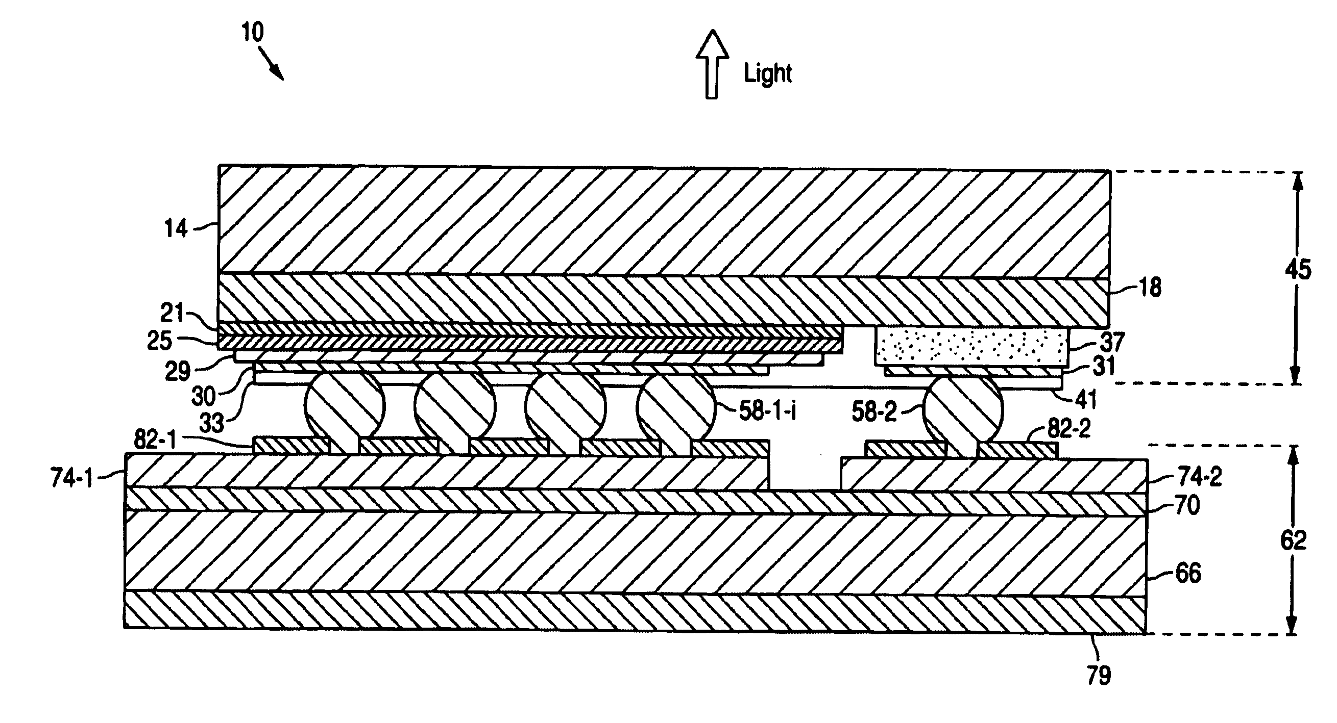
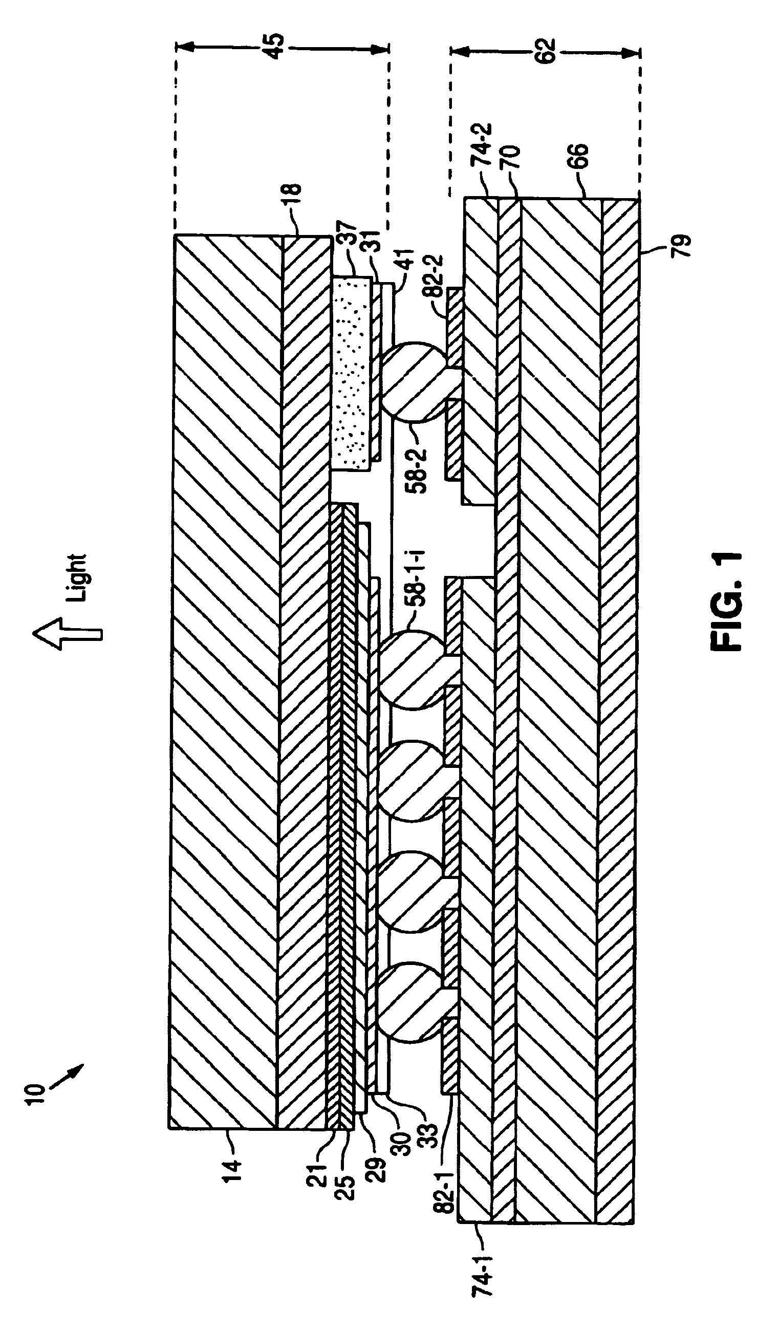
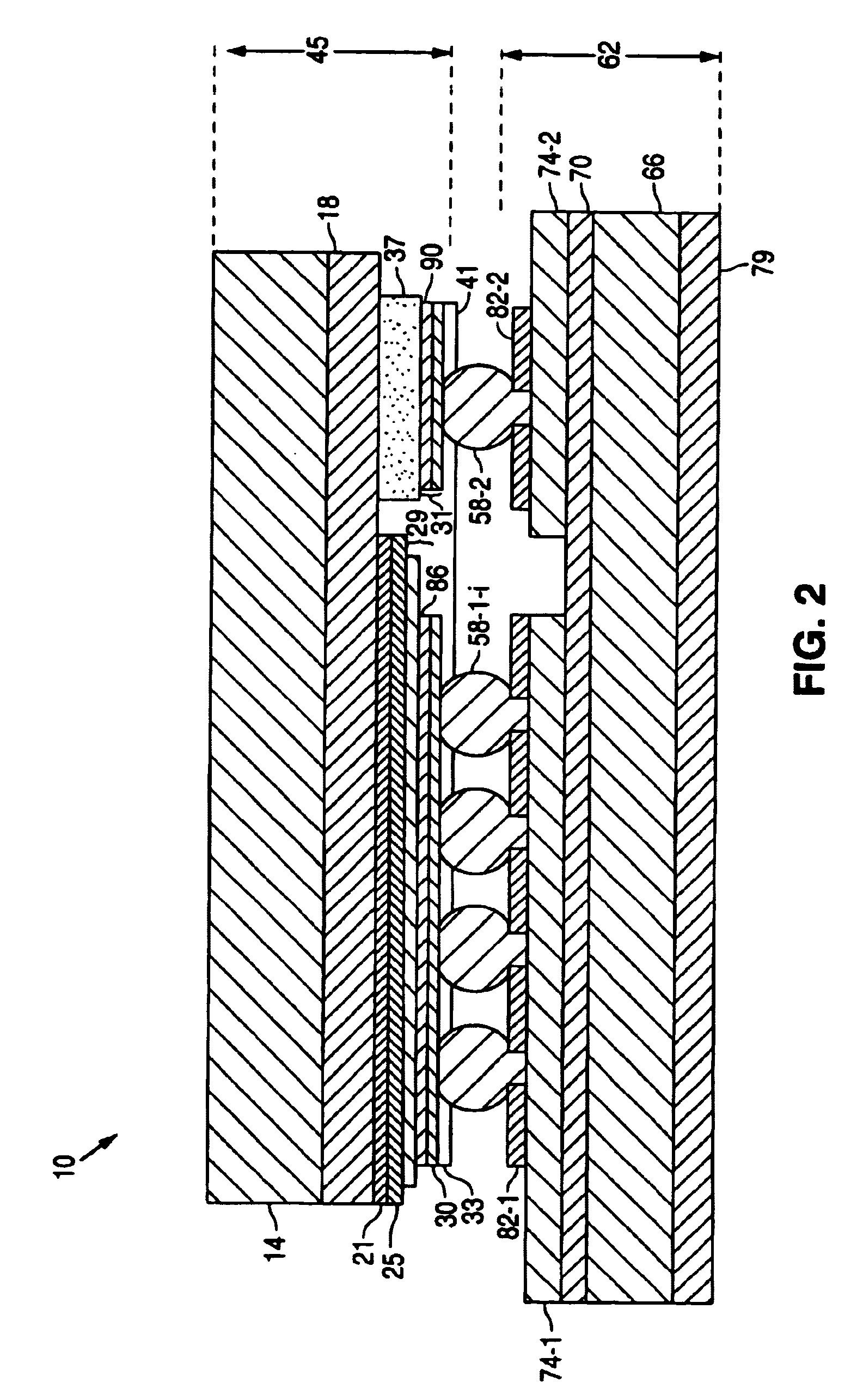
[0016]FIG. 1 illustrates a III-nitride flip chip light emitting device according to embodiments of the present invention. Aspects of the flip chip design illustrated in FIG. 1 are described in more detail in U.S. Pat. No. 6,486,499, issued Nov. 26, 2002, titled “III-Nitride Light-Emitting Device With Increased Light Generating Capability,” and incorporated herein in its entirety by this reference. In flip chip 10, die 45 is manufactured, then flipped and mounted on submount 62 such that light is extracted from the device through growth substrate 14. The manufacture of the flip chip light emitting diode 10 starts with the die 45. Die 45 is manufactured initially by epitaxially depositing semiconductor material on a substrate by molecular beam epitaxy, metal-organic chemical vapor deposition, or any other suitable epitaxial technique. Metals are then deposited and patterned on the semiconductor material to form contacts. An interconnect material is then used to connect the submount 62...


PUM


Abstract

A light emitting device includes a first semiconductor layer of a first conductivity type, an active region, and a second semiconductor layer of a second conductivity type. First and second contacts are connected to the first and second semiconductor layers. In some embodiments at least one of the first and second contacts has a thickness greater than 3.5 microns. In some embodiments, a first heat extraction layer is connected to one of the first and second contacts. In some embodiments, one of the first and second contacts is connected to a submount by a solder interconnect having a length greater than a width. In some embodiments, an underfill is disposed between a submount and one of the first and second interconnects.

Description

BACKGROUND[0001]1. Field of Invention[0002]The present invention relates to high-powered light emitting diodes, more particularly to improving the thermal properties of high-powered light emitting diodes with flip-chip architecture.[0003]2. Description of Related Art[0004]Light emitting diodes (“LEDs”) are solid-state light sources with multiple advantages. They are capable of providing light with high brightness reliably and thus find applications in displays, traffic lights, and indicators, among others. An important class of light emitting diodes is fabricated from one or more Group III elements, such as gallium, indium, or aluminum, and the group V element of nitrogen. These “III-nitride” LEDs are capable of emitting light in the green, blue, or even ultraviolet regime of the spectrum, and thus have many promising applications. Other suitable materials systems for fabrication of light emitting diodes include the III-phosphide, III-arsenide and II-VI materials systems.[0005]LEDs ...

Claims


Application Information

Patent Timeline
IPC IPC(8): H01L33/38H01L33/62
CPCH01L33/38H01L33/62H01L24/17H01L33/20H01L2224/16H01L2924/01079H01L2924/01019H01L2924/12041H01L2924/01012H01L2924/01029H01L2224/05568H01L2224/05023H01L2224/05001H01L2924/00014H01L2224/16237H01L24/05H01L24/16H01L2224/0603H01L2224/131H01L2224/05599H01L2224/05124H01L2224/05139H01L2224/05144H01L2224/05147H01L2924/014
Inventor SHEN, YU-CHENSTEIGERWALD, DANIEL A.MARTIN, PAUL S.
Owner LUMILEDS
Why Eureka
Try Eureka