Manufacturing method for semiconductor device having a T-type gate electrode

Inactive Publication Date: 2005-12-27
LAPIS SEMICON CO LTD
View PDF17 Cites 4 Cited by
  • Summary
  • Abstract
  • Description
  • Claims
  • Application Information

AI Technical Summary

Benefits of technology

[0012]It is preferable that a condition for etching the first insulating film is that the second insulating film is hardly etched. It is thereby possible to etch the first insulating film using the second insulating film as a mask.
[0013]It is also preferable that the second polysilicon is undoped polysilicon. With the undoped silicon, it is possible to prevent impurities from hampering a silicide reaction during siliciding.
[0014]In the method for manufacturing the polysilicon gate including

Problems solved by technology

The impurities thus injected hamper a silicide reaction and prevents the resistance of the gate from decreasing.
In addition, the resistances of the gates of the transistors are irregular, thereby making it disad

Method used


Image

  • Manufacturing method for semiconductor device having a T-type gate electrode
  • Manufacturing method for semiconductor device having a T-type gate electrode
  • Manufacturing method for semiconductor device having a T-type gate electrode

Examples


first embodiment

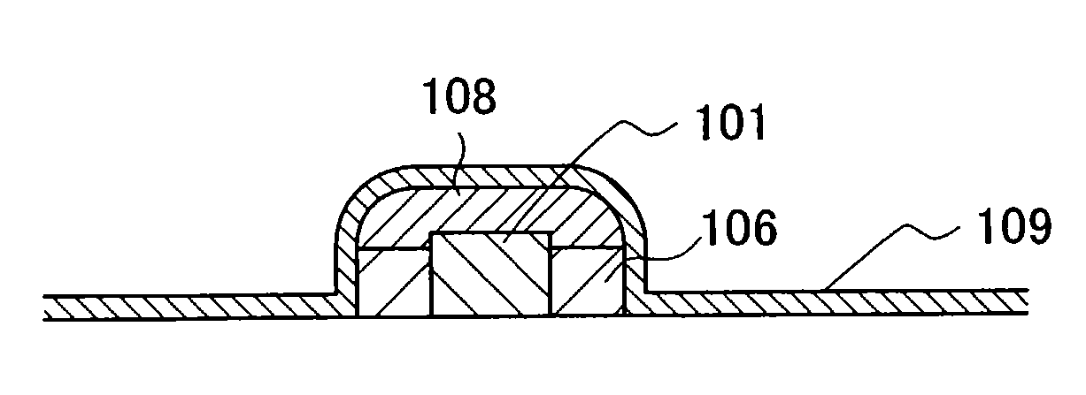
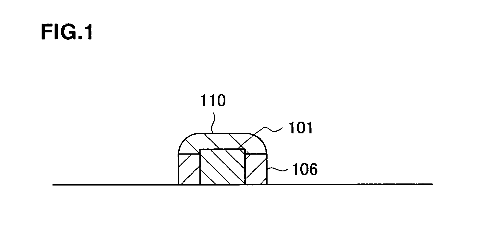
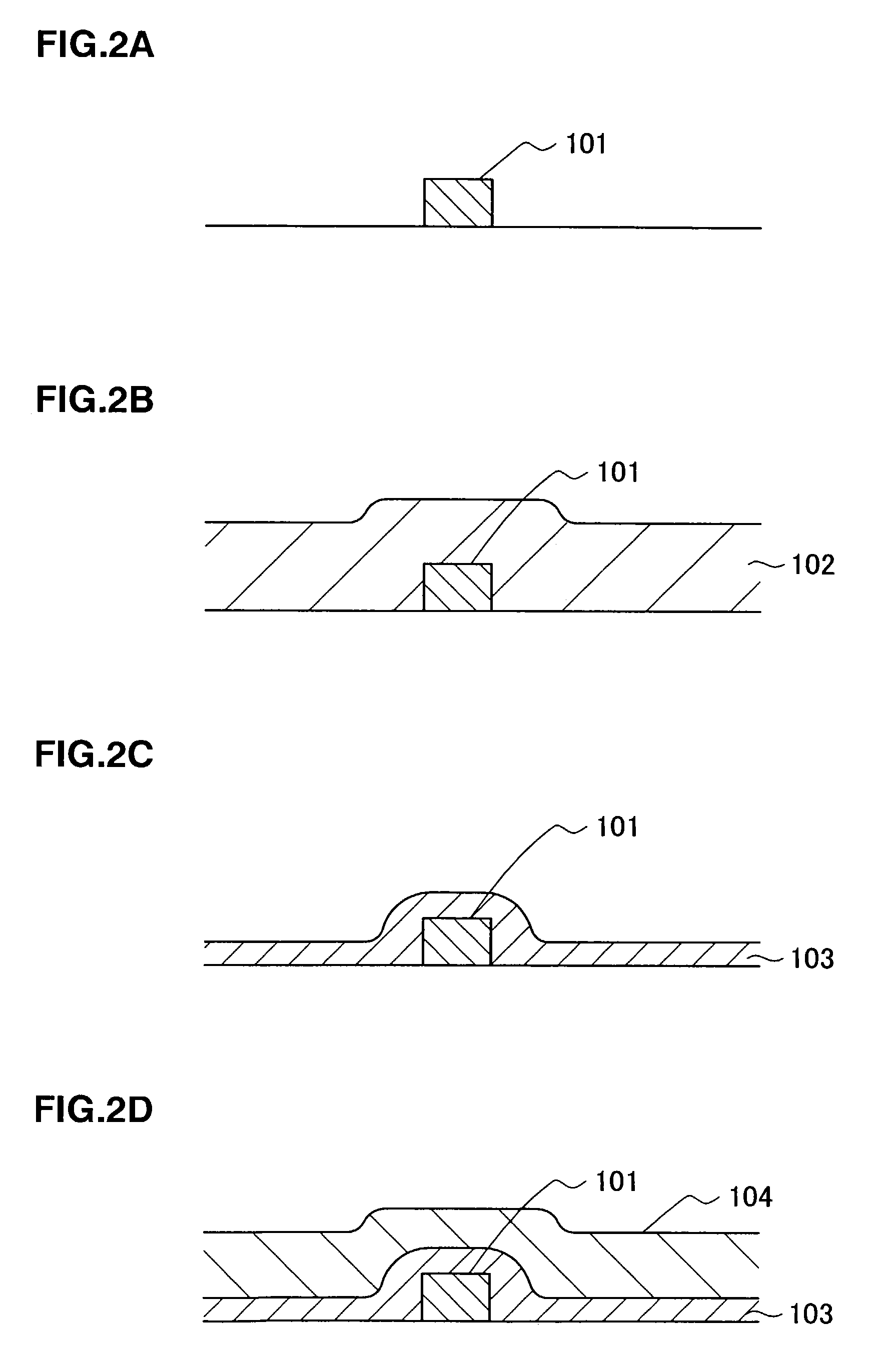
[0019]FIG. 1 is a cross-sectional view of a gate portion formed in the first embodiment. FIGS. 2A to 2J are cross-sectional views showing the steps of forming the gate shown in FIG. 1.

[0020]Impurities (not shown) are injected first into an element formation region on a semiconductor substrate made of, for example, silicon so as to obtain a desired threshold voltage (Vt). A photolithographic step, an etching step and the other step are executed, whereby first polysilicon, e.g., rectangular gate polysilicon 101 (FIG. 2A) is formed as a lower gate having a design gate length (about 0.15 μm). The height of the gate polysilicon is preferably about 150 nm.

[0021]Thereafter, in order to obtain an LDD (Lightly Doped Drain) structure which can decrease leak current and improve reliability, impurities are injected into source and drain regions with the gate polysilicon 101 used as a mask to thereby form, for example, a low concentration, shallow n type layer (not shown).

[0022]Next, a nitride f...

second embodiment

[0031]FIGS. 3A to 3J show cross-sectional views showing the steps of forming a gate portion in the second embodiment according to the present invention.

[0032]Similarly to the first embodiment, first polysilicon having a design gate length, e.g., rectangular gate polysilicon 201 having a gate length of about 150 nm is formed as a lower gate electrode (FIG. 3A). Thereafter, in order to obtain the LDD structure, impurities are injected into source and drain regions with the gate polysilicon 201 used as a mask to thereby form, for example, a low concentration n type layer (not shown).

[0033]Next, a nitride film 202, for example, is formed as the first insulating film on the entire surface of the substrate so as to cover the gate polysilicon 201 by a CVD method (FIG. 3B). In this case, the nitride film 202 is formed to set the thickness thereof to be larger than the height of the gate polysilicon 201 and to leave the difference in height around the gate polysilicon 201. The thickness of t...


PUM


Abstract

This invention provides a semiconductor device manufacturing method including forming a T type gate electrode having a wide region in an upper portion, the method including steps of: forming rectangular gate polysilicon; forming a nitride film covering the polysilicon; forming an oxide film thick on the nitride film; etching back the oxide film to expose the nitride film; etching the exposed nitride film, exposing the gate polysilicon, and forming a space; forming undoped polysilicon burying the space; etching back the undoped polysilicon to form a wide portion in the upper portion of the gate polysilicon; and etching the oxide film and the nitride film; siliciding the wide undoped silicon to form titanium suicide (or cobalt silicide). This manufacturing method makes it possible to easily form the T type gate electrode with good yield.

Description

BACKGROUND OF THE INVENTION[0001]The present invention relates to a method for manufacturing a semiconductor device having a T type gate electrode, and particularly relates to a semiconductor device manufacturing method which can prevent an increase in the resistance of the suicide gate of a transistor following the thinning of the suicide gate.DESCRIPTION OF THE RELATED ART[0002]As a method for preventing an increase in the resistance of the gate of a transistor following the thinning of the gate, a method for forming a gate to have an upper portion of the gate widened or forming a so-called T-type gate electrode is disclosed by Japanese Patent Laid-Open Publication Nos. 2000-36594 and 5-63002.[0003]Recently, as the performances of semiconductor devices increase, transistor gates are increasingly made thinner. According to a conventional method for forming a titanium silicide gate or a cobalt silicide gate, a rectangular gate is formed first by polysilicon and a nitride film is the...

Claims


Application Information

Patent Timeline
IPC IPC(8): H01L21/28H01L21/336H01L29/423H01L29/49H01L29/78
CPCH01L21/28114H01L29/42376H01L29/665
Inventor SUZUKI, SO
Owner LAPIS SEMICON CO LTD
Why Eureka
Try Eureka