Method of making a dual GMR read head with self-pinned layer and specular reflector

a self-pinned layer and read head technology, applied in the field of dual-spin valve sensor with self-pinned layer and specular reflector, can solve the problems of thin self-pinned layer not providing an adequate boundary. , to achieve the effect of reducing the magnetoresistive coefficient (dr/r), reducing the number of conduction electrons in the mean free path

Inactive Publication Date: 2006-01-10
HITACHI GLOBAL STORAGE TECH NETHERLANDS BV
View PDF1 Cites 13 Cited by
  • Summary
  • Abstract
  • Description
  • Claims
  • Application Information

AI Technical Summary

Benefits of technology

[0009]The present invention provides a novel dual spin valve sensor which is thinner than prior art dual spin valve sensors. The present dual spin valve sensor may be the same as the aforementioned dual spin valve sensor except one of the pinned layer structures is a self-pinned layer which is located between a specular reflector structure and one of the spacer layers. The magnetic moment of the self-pinned layer is not pinned by an antiferromagnetic pinning layer but, in contrast, the magnetic moment is pinned by sense current fields from other layers in the spin valve sensor when the sense current is conducted through the spin valve sensor. In order for this to occur the thickness of the self-pinned layer should be maintained below 15 Å with a preferable thickness of 10 Å. The reason for this is because the thicker the self-pinned layer the greater the sense current fields that are required to pin the magnetic moment of the self-pinned layer. Unfortunately, when the self-pinned layer is thin there is a scattering of conduction electrons at a boundary of the self-pinned layer, which reduces the number of conduction electrons in the mean free path which, in turn, reduces the magnetoresistive coefficient (dr / R). The ideal situation is for the scattering events of the conduction electrons in the mean free path to be in phase. When there is scattering at a boundary of the mean free path this is referred to in the art as inelastic scattering which causes the scattering events to be out of phase and to work against one another to reduce the magnetoresistive coefficient (dr / R). Accordingly, a thin self-pinned layer does not provide an adequate boundary for the mean free path to prevent boundary scattering of conduction electrons.

Problems solved by technology

Unfortunately, when the self-pinned layer is thin there is a scattering of conduction electrons at a boundary of the self-pinned layer, which reduces the number of conduction electrons in the mean free path which, in turn, reduces the magnetoresistive coefficient (dr / R).
Accordingly, a thin self-pinned layer does not provide an adequate boundary for the mean free path to prevent boundary scattering of conduction electrons.

Method used


Image

  • Method of making a dual GMR read head with self-pinned layer and specular reflector
  • Method of making a dual GMR read head with self-pinned layer and specular reflector
  • Method of making a dual GMR read head with self-pinned layer and specular reflector

Examples


first embodiment

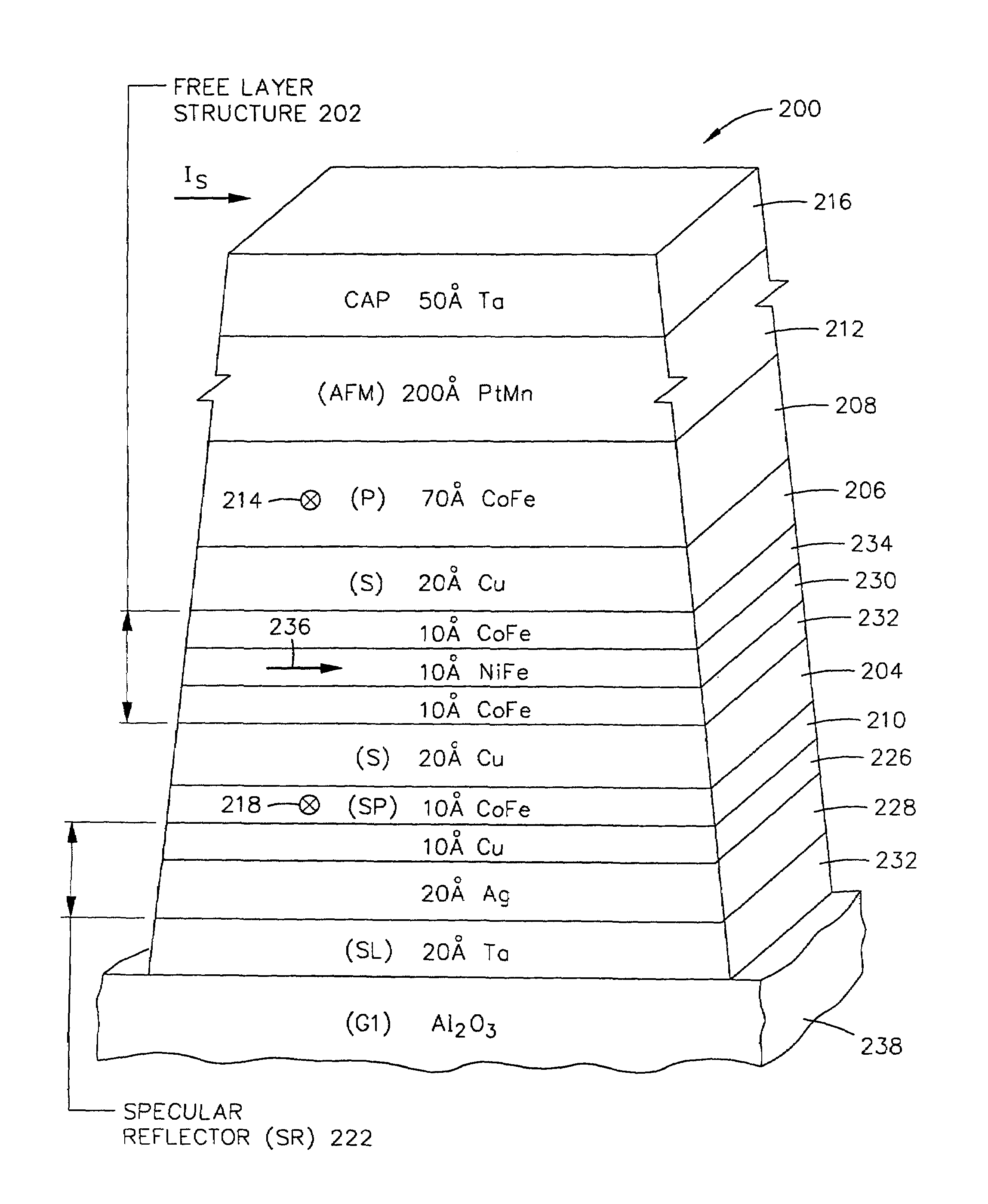
[0039]the present dual spin valve sensor 200 is illustrated in FIGS. 12 and 13. The sensor 200 includes a ferromagnetic free layer structure 202 which is located between nonmagnetic conductive first and second spacer layers (S) 204 and 206. The designation of first and second layers throughout the description has no significance regarding their respective locations which means that the spacer layer 206 could be the first spacer layer and the spacer layer 204 could be the second spacer layer. The first and second spacer layers 204 and 206 are located between a pinned layer structure (P), which is preferably a single pinned layer 208, and a self-pinned layer (SP) 210 respectively. The pinned layer 208 is exchange coupled to an antiferromagnetic (AFM) pinning layer 212 which pins a magnetic moment 214 of the pinned layer perpendicular to the ABS in a direction toward the ABS or away from the ABS, as shown in FIG. 12. A cap layer 216 may be on the pinning layer 212 for protecting it fro...

second embodiment

[0048]the present dual spin valve sensor 300 is illustrated in FIGS. 14 and 15. The dual spin valve sensor 300 is the same as the spin valve sensor 200 illustrated in FIGS. 12 and 13 except an antiparallel (AP) pinned layer structure 302 has been substituted for the pinned layer 208, the second specular reflector layer 228 may optionally be gold (Au), the seed layer 232 may optionally be nickel manganese oxide (NiMnO) or zirconium (Zr), and the first specular reflector layer 226 may be composed of an alloy of copper (Cu) and X where X is a high resistance material such as nickel (Ni), zirconium (Zr) or chromium (Cr) for reducing shunting of the sense current through the first specular reflector structure 222. The AP pinned layer structure 302 includes an antiparallel coupling layer 304 which is located between first and second ferromagnetic antiparallel layers (AP1) and (AP2) 306 and 308. The first antiparallel layer 306 is exchange coupled to the antiferromagnetic pinning layer 212...

third embodiment

[0051]the present spin valve sensor 400 is shown in FIGS. 16 and 17. This spin valve sensor is the same as the spin valve sensor 200 shown in FIG. 12 except all of the layers of the spin valve sensor have been reversed or turned upside down except for the seed layer 232 and the cap layer 216. This type of spin valve sensor is referred to in the art as a bottom spin valve sensor since the antiferromagnetic pinning layer 212 is now located at the bottom instead of at the top. It should be noted that the sense current IS now causes the magnetic moment 218 of the self-pinned layer to be toward the ABS instead of away from the ABS. Accordingly, the magnetic moment 214 of the pinned layer 208 should be pinned perpendicular to and toward the ABS by the antiferromagnetic pinning layer 212 so that the magnetic moments 214 and 218 are parallel with respect to one another. With the magnetic moment 236 of the free layer structure parallel to the ABS, as shown in FIGS. 16 and 17, a rotation upwa...


PUM

PropertyMeasurementUnit
thicknessaaaaaaaaaa
nonmagneticaaaaaaaaaa
nonmagnetic conductiveaaaaaaaaaa

Abstract

A dual GMR or dual spin valve sensor has a self-pinned layer which has its magnetic moment pinned perpendicular to an air bearing surface by sense current fields from conductive layers in the dual spin valve sensor when a sense current is conducted therethrough. This scheme eliminates one of the antiferromagnetic pinning layers which is typically employed in a dual GMR or dual spin valve sensor. The self-pinned layer is thin so that its demagnetization field will not be greater than the sense current fields acting thereon. Because of the thinning of the self-pinned layer the spin valve effect of the spin valve sensor is degraded by scattering of conduction electrons at the boundary of the self-pinned layer. In order to overcome this problem a specular reflector layer is employed in contact with the self-pinned layer for reflecting the conduction electrons back into a mean free path of conduction electrons so that the spin valve effect on the self-pinned layer side of the spin valve sensor can be added to another spin valve effect on the other side of the free layer structure for providing a double spin valve effect with an improved read gap, as compared to prior art dual spin valve sensors.

Description

REFERENCE TO RELATED APPLICATIONS[0001]This application is a divisional application of Ser. No. 09 / 760,937, filed on Jan. 16, 2001 and now U.S. Pat. No. 6,655,008, which is a divisional application of 09 / 344,817, filed on Jun. 25, 1999 and now U.S. Pat. No. 6,219,208.BACKGROUND OF THE INVENTION[0002]1. Field of the Invention[0003]The present invention relates to a dual spin valve sensor with a self-pinned layer and a specular reflector and, more particularly, to a read head that produces a double spin valve effect with a pinned layer structure and self-pinned layer wherein the pinned layer structure is pinned by a pinning layer and the self-pinned layer is pinned by sense current fields and interfaces a specular reflector layer for reflecting conduction electrons into the mean free path of conduction electrons.[0004]2. Description of the Related Art[0005]An exemplary high performance read head employs a spin valve sensor for sensing magnetic fields on a moving magnetic medium, such ...

Claims


Application Information

Patent Timeline
Patent Type & Authority Patents(United States)
IPC IPC(8): G11B5/187G11B5/39
CPCB82Y10/00B82Y25/00G11B5/3903G11B5/3954G11B5/3932Y10T29/4906G11B2005/3996Y10T29/49044Y10T29/49043Y10T29/49032G11B5/3967
Inventor GILL, HARDAYAL SINGH
Owner HITACHI GLOBAL STORAGE TECH NETHERLANDS BV
Why Eureka
Try Eureka