Integrated antenna device with resistive connection

a resistive connection and antenna technology, applied in the direction of waveguide type devices, resonance antennas, radiating element structural forms, etc., can solve the problems of devices with good yield, achieve the effect of low resistivity, improve the effect of robustness and reproducibility, and reduce the resistance of the antenna

Inactive Publication Date: 2006-01-24
QINETIQ LTD +1
View PDF4 Cites 10 Cited by
  • Summary
  • Abstract
  • Description
  • Claims
  • Application Information

AI Technical Summary

Benefits of technology

[0012]Since the connection structure is small scale—the tracks are of small width and lateral spacing—at high frequency, the subdivided connection is the equivalent of a uniform resistive sheet. The connection may thus be provided f...

Problems solved by technology

It is a problem producing resistive connections of high sheet resisti...

Method used


Image

  • Integrated antenna device with resistive connection
  • Integrated antenna device with resistive connection
  • Integrated antenna device with resistive connection

Examples


Embodiment Construction

[0020]Embodiments of the invention will now be described, by way of example only, and with reference to the accompanying drawings.

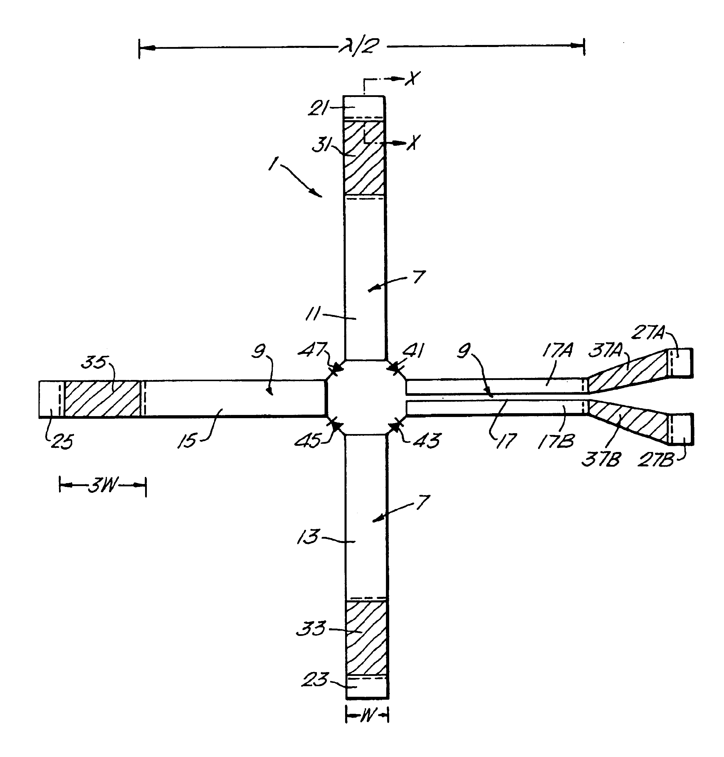
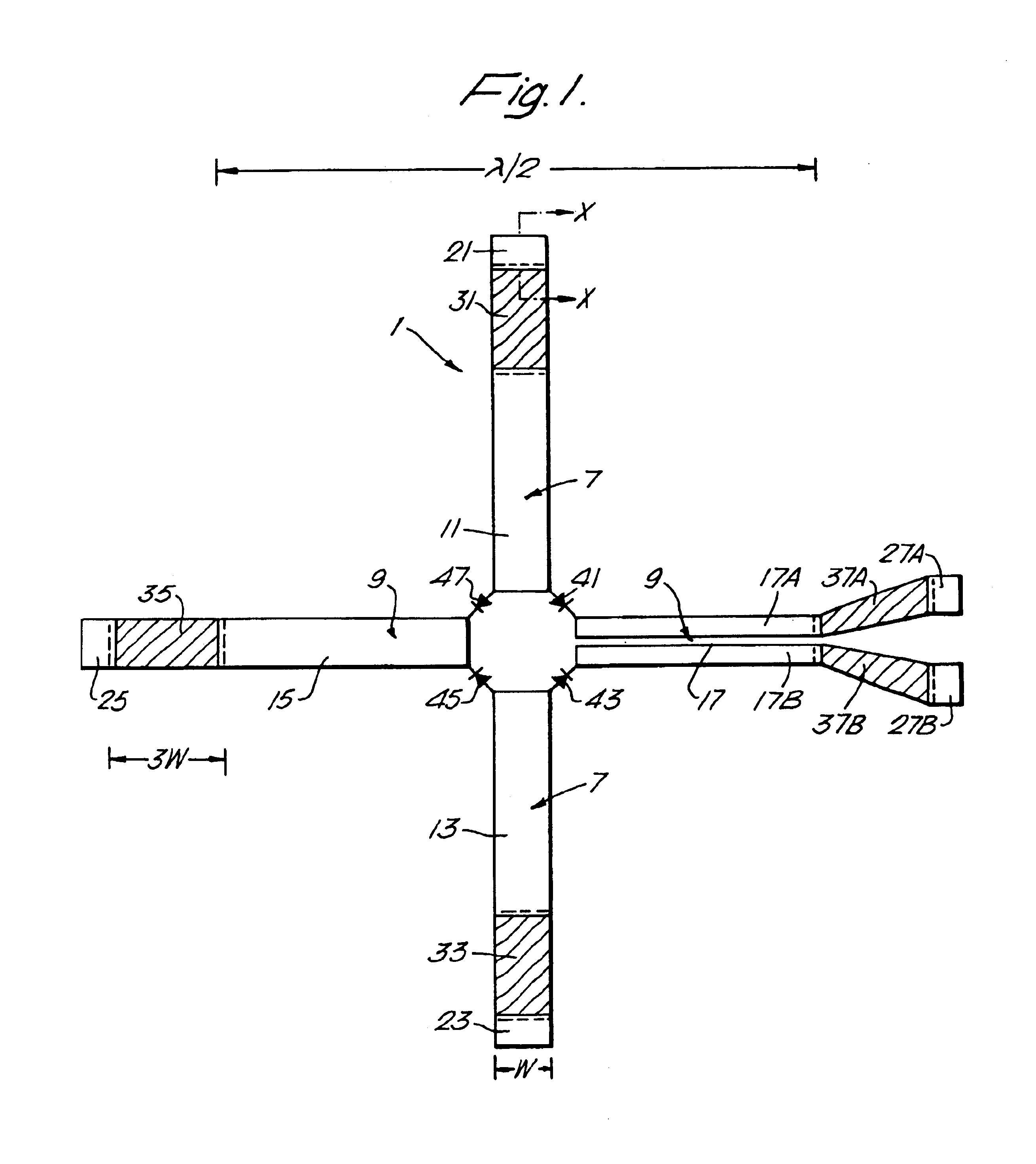
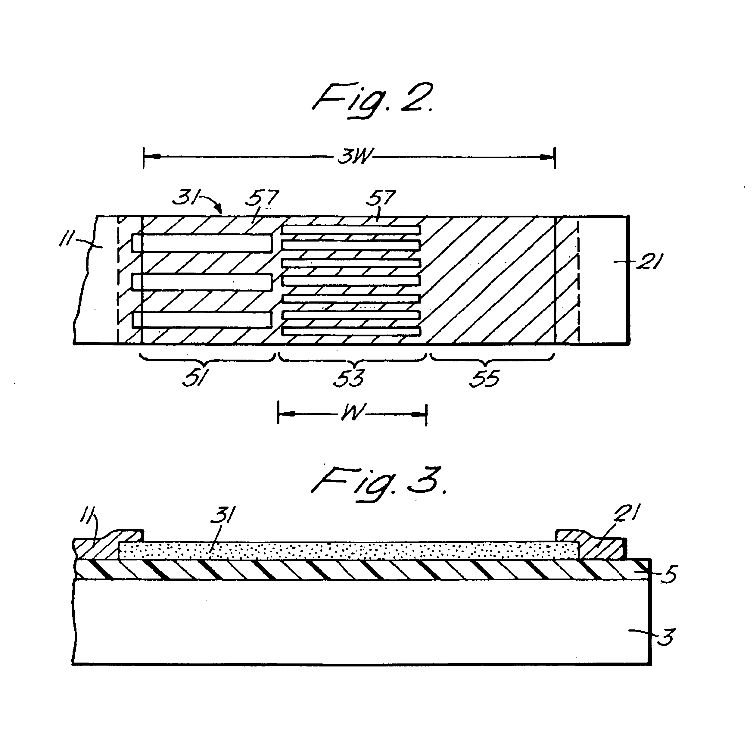
[0021]In FIG. 1, the integrated antenna-receiver shown comprises a planar metal antenna 1 mounted on a supporting body 3, a substrate of semiconductor material, silicon. Insulation between the antenna metal and the semiconductor material is provided by a thin spacing layer 5 of dielectric material—thermally grown silicon dioxide. This prevents the formation of intermetallic compounds between the antenna and the semiconductor.

[0022]The planar metal antenna 1 comprises two orthogonal dipoles 7 and 9, each of which is defined by a pair of metal strip limbs—limbs 11, 13 and limbs 15, 17 respectively. One of the four limbs, limb 17, is divided along its length into two portions 17A and 17B. These portions 17A and 17B are isolated at low frequency, but at high frequency they are strongly coupled and behave together as a single limb. Corresponding to each limb t...


PUM


Abstract

A planar metal antenna mounted on a semiconductor body and incorporating an active circuit element, for example a diode, integrated in the path of the antenna. Connection between the antenna metal and a peripheral contact is provided by a connecting link of resistive sheet material sub-divided, by voids or by inclusions of high resistive material, into a number of conductive tracks each of width and spacing of dimension small compared with the width of the antenna. The link thus exhibits an effectively high sheet resistivity at high frequency—i.e. at a frequency at or near to the frequency of antenna resonance and thus affords effective hf isolation between the antenna and the contact. At the same time, at dc and at intermediate frequency, a relatively low resistance path is afforded for bias and for extraction of IF signal. The number, width and spacing of the tracks may be varied with distance from the antenna metal to minimize the dc resistivity. Thus the track density may be graded; the link may be comprised of several sections each of different track density. Alternatively, the track density may be made a tapered function of distance from the antenna metal by variation of the size and density of voids or high resistivity inclusions. The connection may be formed of material overlying the semiconductor body. Alternatively, it may be defined in the semiconductor body by dopant implant.

Description

TECHNICAL FIELD[0001]The present invention concerns an integrated antenna device—for example an integrated antenna-receiver—a device having a body of semiconductor material, a planar metal antenna supported on the body, and one or more circuit elements incorporated in the semiconductor body, elements integrated with the metal antenna. Resistive connection is provided between the antenna device and corresponding contacts located remote from the antenna metal, to facilitate the coupling of the device to operative components—for example to power source or bias supply components, components external to the device, or to input control circuitry or output processing circuitry—components external to the device or incorporated in the semiconductor body at locations remote from the antenna metal.BACKGROUND[0002]Integrated antenna-receivers, and antenna-transmitters, for millimetre-band, have been discussed in Electronics Letters Vol. 17 No 20 pages 729-730 (October 1981). This article refers...

Claims


Application Information

Patent Timeline
IPC IPC(8): H01Q1/00H01Q9/16H01P1/00H01Q1/38H01Q3/24H01Q23/00
CPCH01Q1/38H01Q23/00H01Q3/247
Inventor REES, HUW DAVID
Owner QINETIQ LTD
Why Eureka
Try Eureka