Method for forming a semiconductor structure with improved smaller forward voltage loss and higher blocking capability

a semiconductor structure and forward voltage technology, applied in the field of semiconductor technology, can solve the problems of low on-resistance, carrier concentration in the drift region of the mosfet device cannot be reduced, and it is not desirable to increase the dopant concentration

Inactive Publication Date: 2006-01-31
SEMICON COMPONENTS IND LLC
View PDF298 Cites 32 Cited by
  • Summary
  • Abstract
  • Description
  • Claims
  • Application Information

AI Technical Summary

Benefits of technology

[0009]Another embodiment of the invention is directed to a method for forming a field effect transistor comprising: a) providing a semiconductor substrate of a first conductivity type having a major surface, a drift region, and a drain region; b) forming a well region of a second conductivity type in the semiconductor substrate; c) forming a source region of the first conductivity type in the well region; d) forming a source contact layer on the source region; e) forming a gate electrode adjacent to the source region; f) forming a charge control electrode in the drift region, wherein the charge control electrode is adapted to be biased at a different potential than the gate electrode or the source contact layer, and is adapted to control the electric field in the drift region; and g) forming a dielectric material around the charge control electrode.

Problems solved by technology

However, it may not be desirable to increase the dopant concentration, because increasing the dopant concentration reduces the breakdown voltage of the device.
Conversely, the carrier concentration in the drift region of the MOSFET device cannot be reduced to increase the breakdown voltage without also undesirably increasing RDS(on).
While such superjunction transistor devices exhibit high breakdown voltages and low on-resistance, they are difficult to manufacture.
This is difficult to achieve in practice.
In addition, because it is extremely difficult to precisely balance the doping in the composite buffer layer of a superjunction transistor device, the practical maximum electrical field achievable in the composite buffer layer is limited to approximately 2×10⁵ V / cm.

Method used


Image

  • Method for forming a semiconductor structure with improved smaller forward voltage loss and higher blocking capability
  • Method for forming a semiconductor structure with improved smaller forward voltage loss and higher blocking capability
  • Method for forming a semiconductor structure with improved smaller forward voltage loss and higher blocking capability

Examples


Embodiment Construction

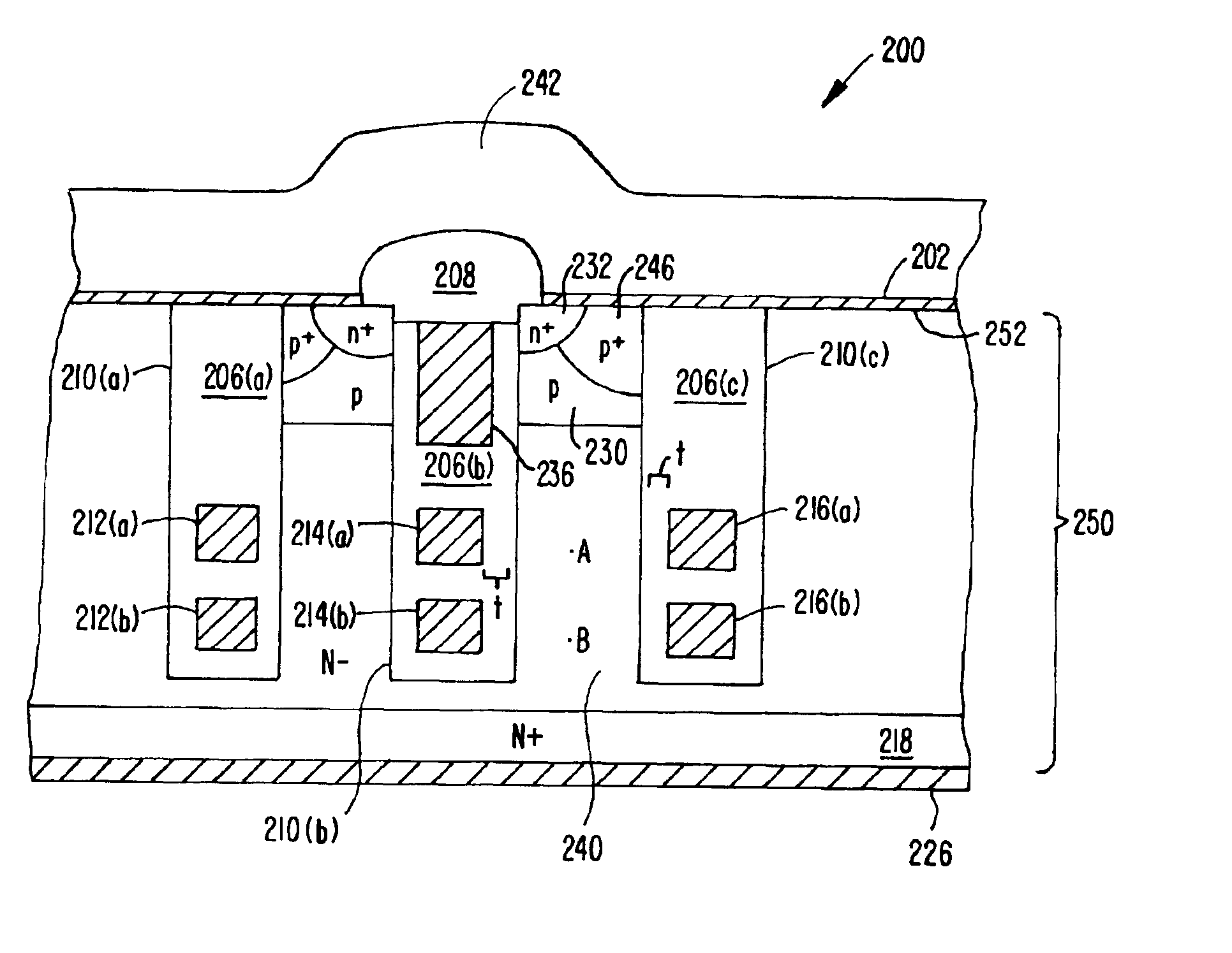
[0020]Embodiments of the invention are directed to semiconductor devices. The semiconductor devices are preferably power semiconductor devices. Examples such semiconductor devices include vertical MOSFETs (e.g., planar gated or trench gated vertical MOSFETs), lateral MOSFETs, bipolar transistors, power diodes, etc.

[0021]The semiconductor devices comprise a semiconductor substrate such as a silicon or gallium arsenide substrate. The semiconductor substrate comprises a region of a first conductivity type (e.g., an N-type region) and can have a major surface. A region of a second conductivity type (e.g., a P-type region) is also formed within the semiconductor substrate.

[0022]In embodiments of the invention, the semiconductor device includes one or more charge control electrodes. The charge control electrodes may be biased with a different potential than the gate, source, and drain to control the electric field within the semiconductor material. In some embodiments, these charge contro...


PUM


Abstract

A semiconductor device is formed as follows. A semiconductor substrate having a first region of a first conductivity type is provided. A region of a second conductivity type is formed in the semiconductor substrate such that the first and second regions form a p-n junction. First and second charge control electrodes are formed adjacent to but insulated from one of the first and second regions, along a dimension parallel to flow of current through the semiconductor device, wherein the first charge control electrode is adapted to be biased differently than the second charge control electrode.

Description

CROSS-REFERENCE TO RELATED APPLICATIONS[0001]This application is a divisional of and claims priority to U.S. application Ser. No. 09 / 981,583, filed Oct. 17, 2001 now U.S. Pat. No. 6,677,641, entitled “Semiconductor Structure with Improved Smaller Forward Voltage Loss and Higher Blocking Capability”, which disclosure is incorporated herein by reference.FIELD OF THE INVENTION[0002]This invention relates in general to semiconductor technology, and in particular to semiconductor devices and their manufacture.BACKGROUND OF THE INVENTION[0003]In a conventional vertical MOSFET (metal oxide semiconductor field effect transistor) device, it is desirable to minimize the drain-to-source resistance or RDS(on) of the device. RDS(on) is proportional to the amount of power consumed while the MOSFET device is on so that reducing RDS(on) reduces the amount of power consumed by the MOSFET device. RDS(on) could be reduced by increasing the dopant (or carrier) concentration in the drift region of the d...

Claims


Application Information

Patent Timeline
Patent Type & Authority Patents(United States)
IPC IPC(8): H01L21/8238H01L21/331H01L29/06H01L29/08H01L29/40H01L29/417H01L29/732H01L29/78H01L29/861
CPCH01L29/404H01L29/407H01L29/7816H01L29/41766H01L2924/0002H01L2924/00H01L29/73H01L21/18H01L31/119H01L29/739
Inventor KOCON, CHRISTOPHER BOGUSLAW
Owner SEMICON COMPONENTS IND LLC
Why Eureka
Try Eureka