

Semiconductor device with reduced current consumption in standby state
a technology of current consumption and semiconductor devices, applied in semiconductor devices, digital storage, instruments, etc., can solve problems such as increasing the current consumption of the entire device, and achieve the effect of reducing the current consumption
- Summary
- Abstract
- Description
- Claims
- Application Information
AI Technical Summary
Benefits of technology
Problems solved by technology
Method used
Image

Examples
first embodiment
[0076
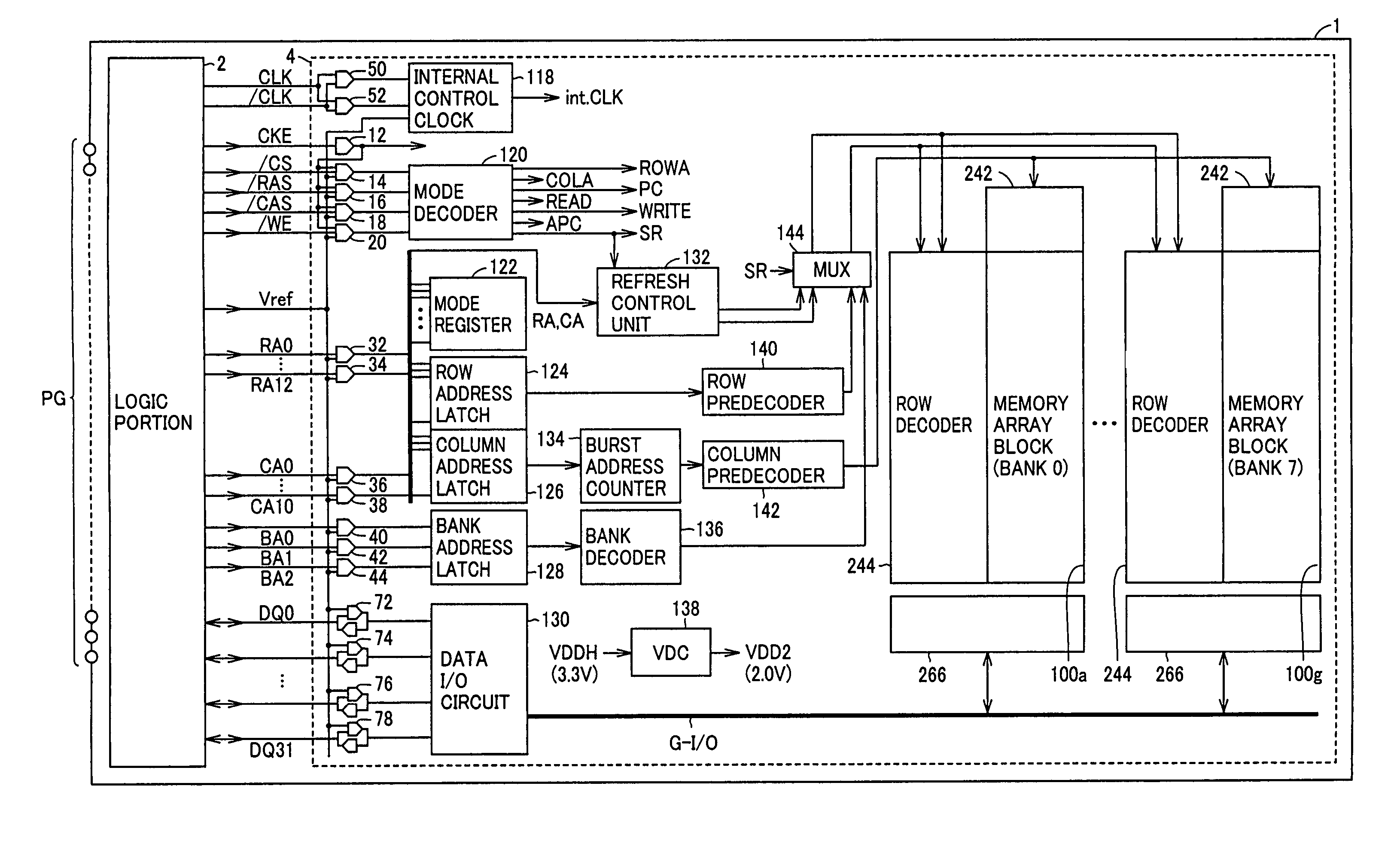
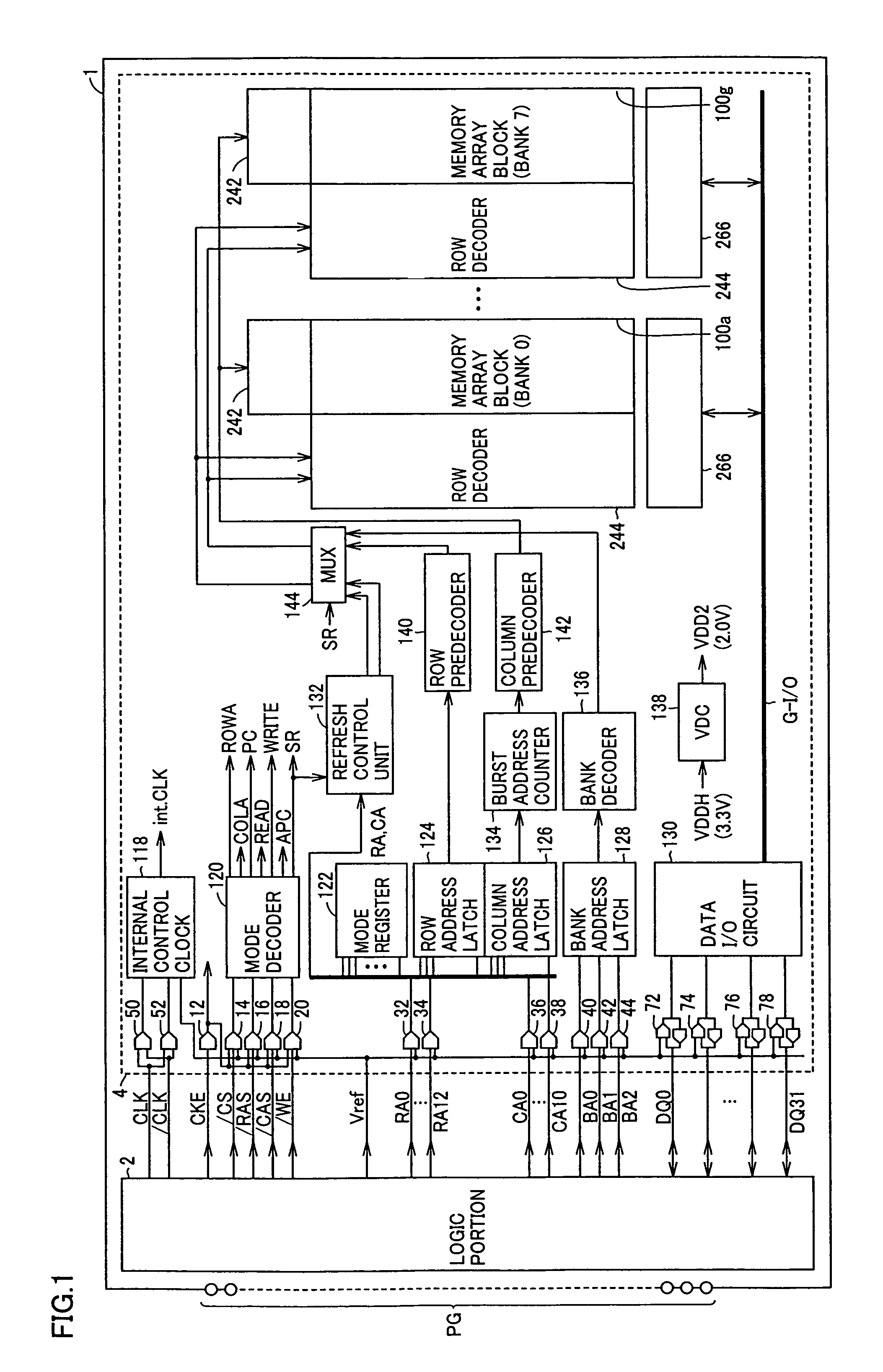
[0077]FIG. 1 is a schematic block diagram showing a structure of a semiconductor device 1 according to the first embodiment of the invention.
[0078]Referring to FIG. 1, semiconductor device 1 includes a large-sized logic portion 2 coupled to a group of external pin terminals PG to carry out designated processing, and a DRAM portion 4 coupled to logic portion 2 via internal interconnection to store data required by logic portion 2. Logic portion 2 outputs to DRAM portion 4, clock signals CLK and / CLK, control signals CKE, / CS, / RAS, / CAS, and / WE, reference potential Vref for taking data in, row address signals RA0–RA12, column address signals CA0–CA10, and bank address signals BA0–BA2. Logic portion 2 and DRAM portion 4 transmit and receive data signals DQ0–DQ31.
[0079]If logic portion 2 and DRAM portion 4 are integrated on one chip, it is easier to increase the number of signal lines for data transmission compared with a logic portion and a DRAM portion mounted on separate chips...
second embodiment
[0149
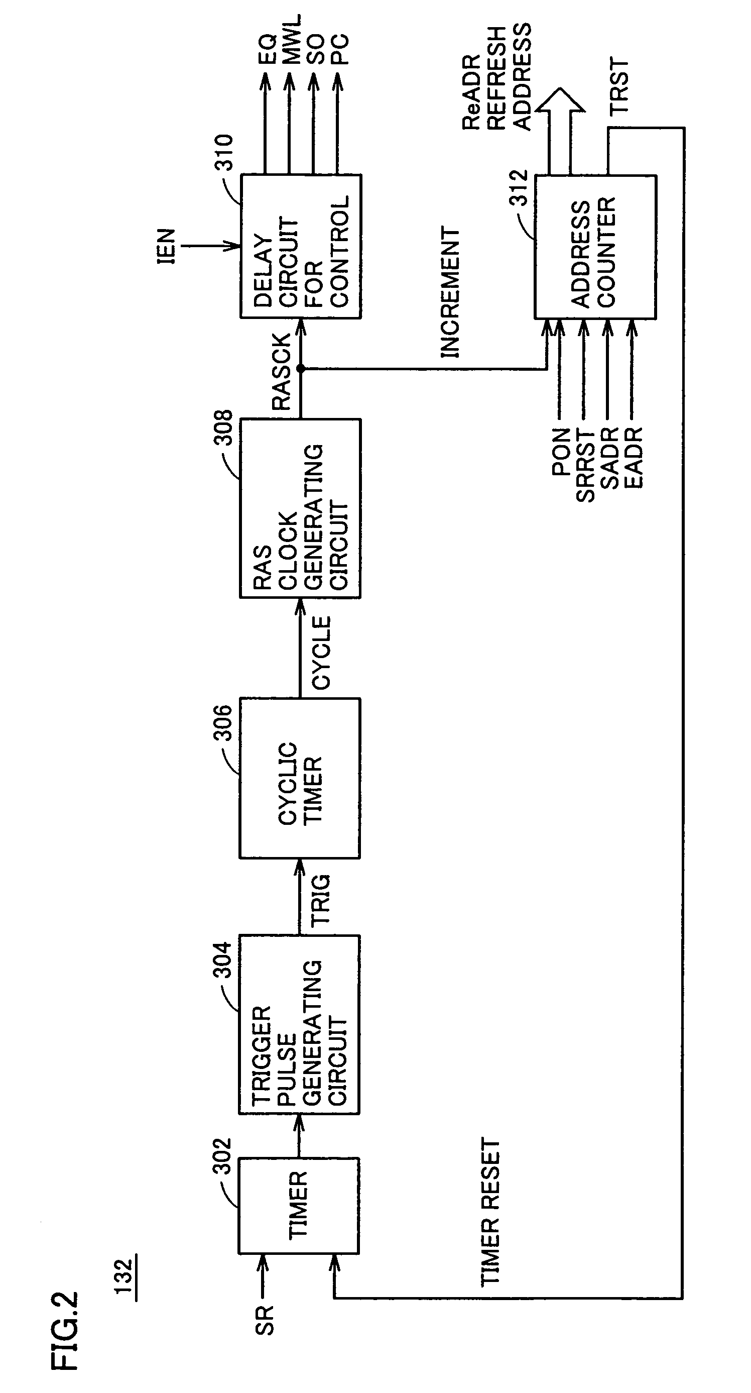
[0150]The first embodiment has been described according to which power consumption is reduced by decreasing the refresh region. It is also possible to cut the power consumption by employing a structure in which power is made off for a certain portion of the internal circuit of the DRAM portion in the power down mode, for example.
[0151]FIG. 9 illustrates that power is externally supplied to a semiconductor device according to the second embodiment.
[0152]Referring to FIG. 9, a semiconductor device CH has a logic portion LG and a DRAM portion MEM. In the DRAM portion, a voltage generating circuit VGEN1 for generating boosted potential VPP and a voltage generating circuit VGEN2 for generating substrate potential VBB are provided.
[0153]Logic portion LG receives supply potential LVDDH of 3.3V via a terminal T1 and receives supply potential VDD of 1.5V via a terminal T2. Supply potential VDD is also applied to DRAM portion MEM. Supply potential DVDDH of 3.3V is applied to DRAM portion...
third embodiment
[0245
[0246]FIG. 30 is a block diagram showing a structure of a semiconductor device 800 according to the third embodiment.
[0247]Referring to FIG. 30, semiconductor device 800 includes a logic portion 802 transmitting and receiving data to and from the outside and performing various arithmetic operations and the like, and a DRAM portion 804 receiving from logic portion 802 a command signal and an address signal and transmitting and receiving data to and from logic portion 802. DRAM portion 804 includes a clock / reset control circuit 806 receiving signal NPDSR from the logic portion and outputting power down mode signal PDSR and making various reset controls, a peripheral circuit 812 receiving a command signal and an address signal from logic portion 802, a peripheral circuit 814 receiving an internal command signal and an internal address signal and the like from peripheral circuit 812 to perform row-related processing, a self refresh control circuit 808 outputting clock signal CLKS t...
PUM
 Abstract
Description
Claims
Application Information