Supercharge Your Innovation With Domain-Expert AI Agents!

Flash EEPROM system with simultaneous multiple data sector programming and storage of physical block characteristics in other designated blocks

a data sector and data sector technology, applied in the direction of memory adressing/allocation/relocation, digital storage, instruments, etc., can solve the problems of increasing power requirements, potential disturbances of adjacent cell charges, and affecting so as to simplify the manufacturing and use of the system, the effect of simplifying the operation of the controller

Inactive Publication Date: 2006-02-07
SANDISK TECH LLC
View PDF111 Cites 21 Cited by
  • Summary
  • Abstract
  • Description
  • Claims
  • Application Information

AI Technical Summary

Benefits of technology

[0008]Multiple user data sectors are programmed into a like number of memory blocks located in different units or sub-arrays of the memory array by alternately streaming data from one of the multiple sectors at a time into the array until a chunk of data is accumulated for each of multiple data sectors, after which the chunks are simultaneously and individually stored in respective blocks in different units of the memory. This increases the number of memory cells that may be programmed in parallel without adverse effects.
[0016]Other characteristics of various memory array circuit chips used to form a system, such as optimal voltage ranges, timing, numbers of pulses used, characteristics of voltage pumps, locations of overhead blocks, and the like, can vary without adverse effects. These operating characteristics can also be tabulated into a single system file for access by the micro-controller, or, more conveniently, the micro-controller can be operated to first access those of such characteristics as are necessary from an individual memory array chip before accessing that chip to read or write data. In either case, this allows the memory system to be formed with memory chips having different characteristics without any degradation in its performance. The manufacturing of non-volatile memory systems is simplified since all the memory array chips in a system need not be the selected to be the same.

Problems solved by technology

Since the programming of data into floating-gate memory cells can take significant amounts of time, a large number of memory cells in a row are typically programmed at the same time.
But increases in this parallelism causes increased power requirements and potential disturbances of charges of adjacent cells or interaction between them.

Method used


Image

  • Flash EEPROM system with simultaneous multiple data sector programming and storage of physical block characteristics in other designated blocks
  • Flash EEPROM system with simultaneous multiple data sector programming and storage of physical block characteristics in other designated blocks
  • Flash EEPROM system with simultaneous multiple data sector programming and storage of physical block characteristics in other designated blocks

Examples


Embodiment Construction

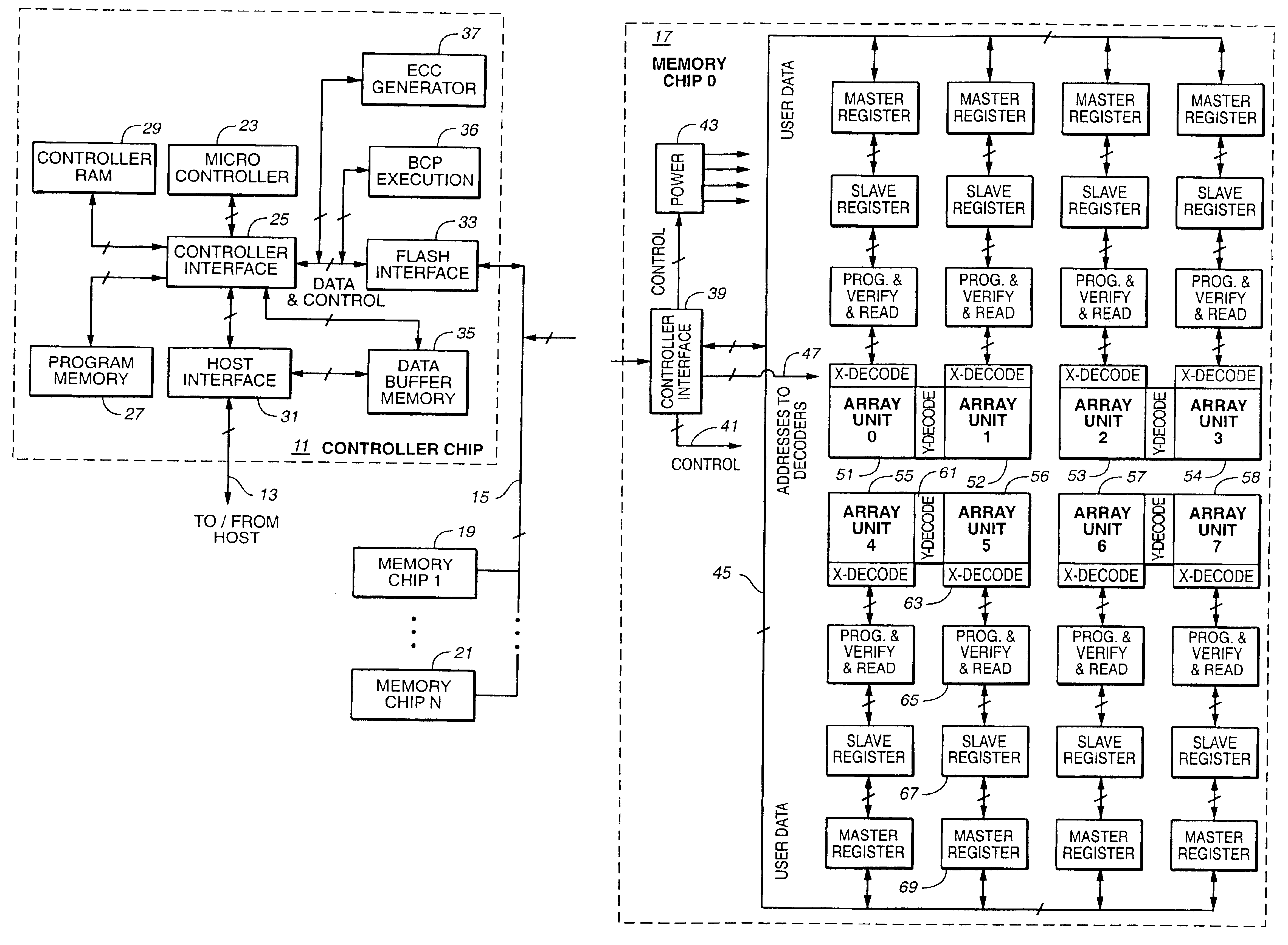
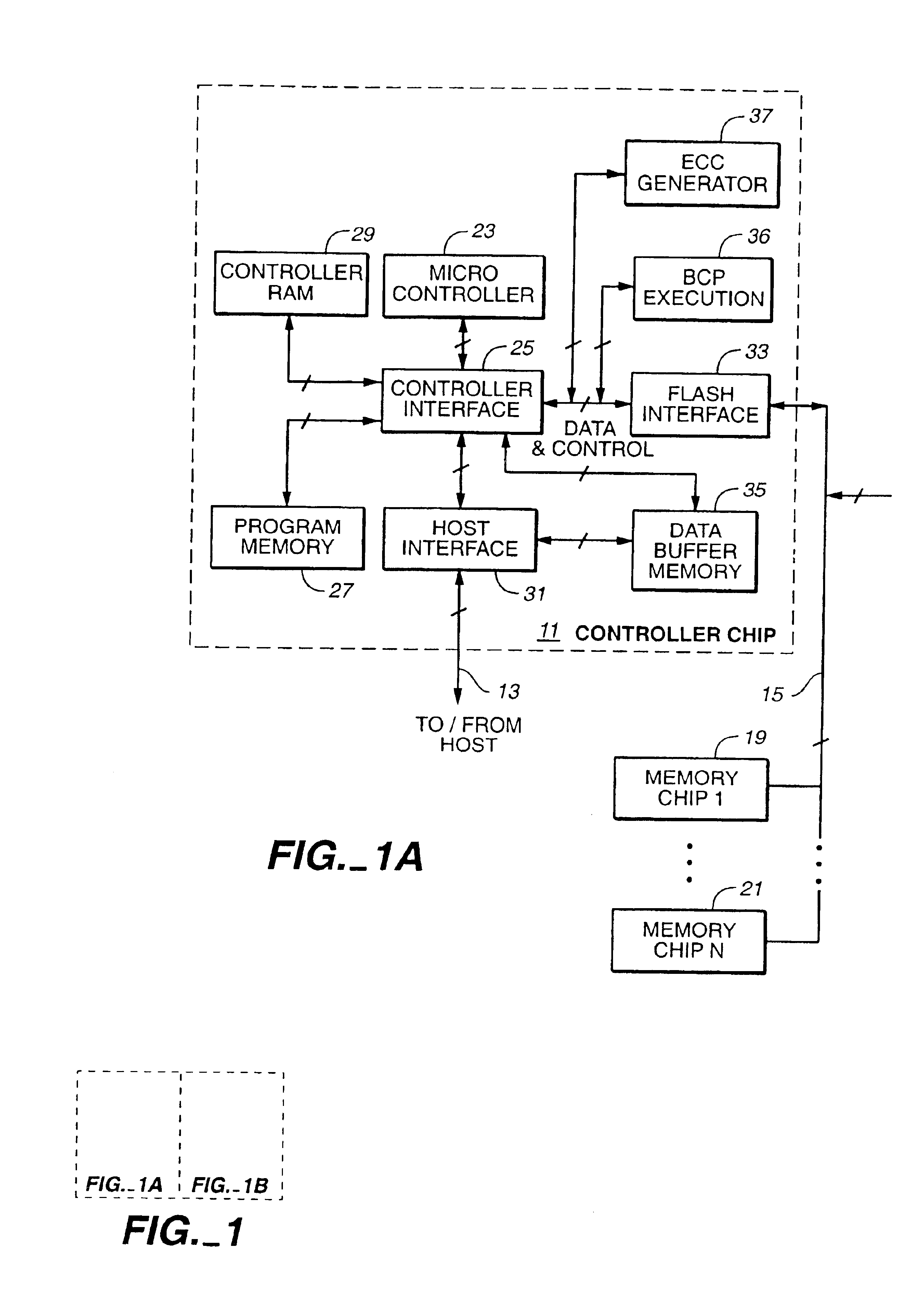
[0037]FIG. 1 provides a diagram of the major components of a non-volatile memory system that are relevant to the present invention. A controller 11 communicates with a host system over lines 13. The controller 11, illustrated to occupy one integrated circuit chip, communicates over lines 15 to one or more non-volatile memory cell arrays, three arrays 17, 19 and 21 being illustrated, each of the arrays usually formed on one or more separate integrated circuit chips. The illustrated controller is usually contained on a single integrated circuit chip, either without a flash EEPROM array (the example shown) or with a memory cell array. Even if a memory cell array is included on the controller circuit chip, an additional one or more chips that each contain only a memory array and associated circuitry will often be included in the system.

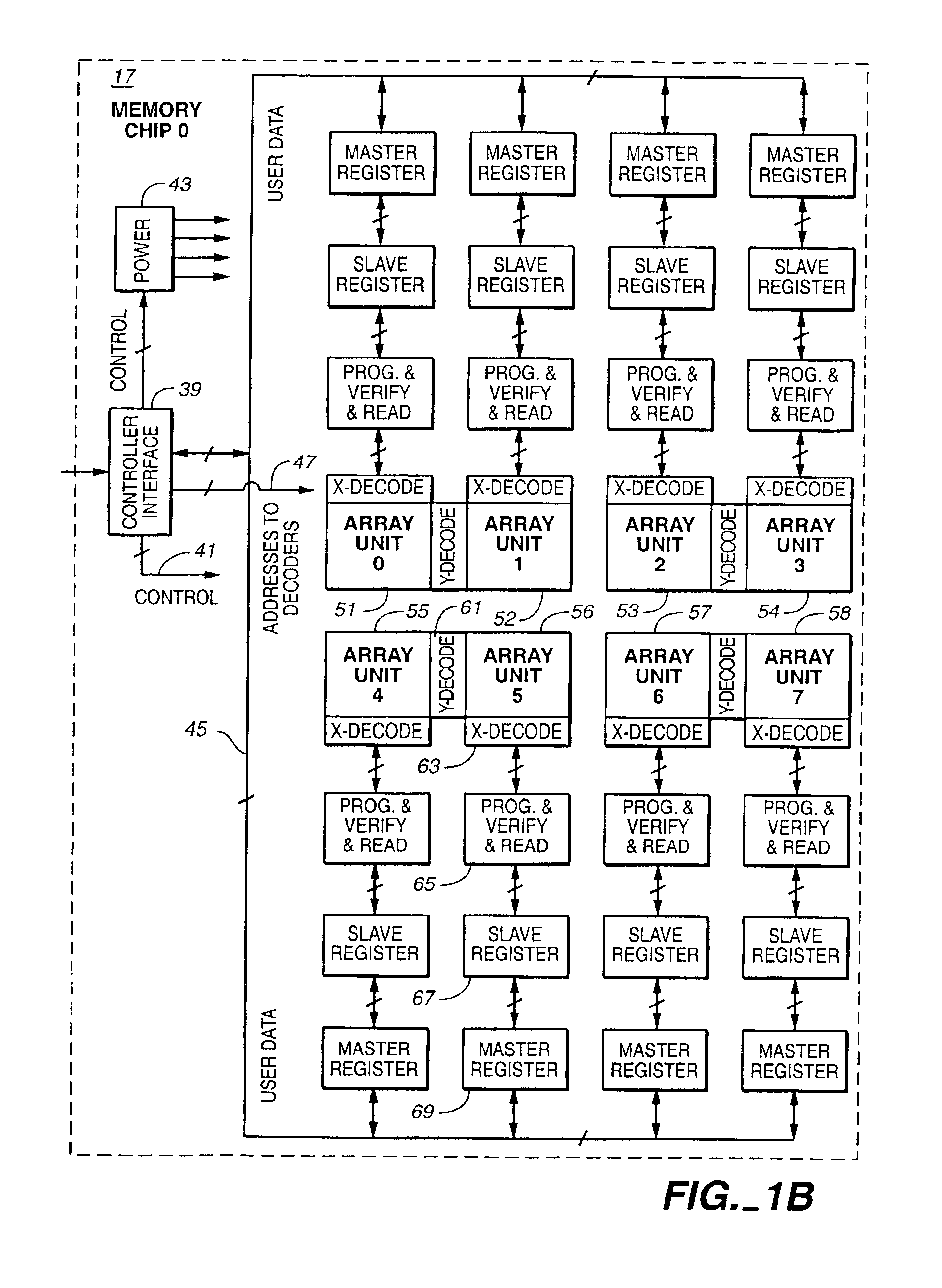
[0038]User data is transferred between the controller 11 and multiple memory arrays 17, 19 and 21, in this example, over the lines 15. The memory arrays ...


PUM


Abstract

A non-volatile memory system is formed of floating gate memory cells arranged in blocks as the smallest unit of memory cells that are erasable together. The system includes a number of features that may be implemented individually or in various cooperative combinations. One feature is the storage in separate blocks of the characteristics of a large number of blocks of cells in which user data is stored. These characteristics for user data blocks being accessed may, during operation of the memory system by its controller, be stored in a random access memory for ease of access and updating. According to another feature, multiple sectors of user data are stored at one time by alternately streaming chunks of data from the sectors to multiple memory blocks. Bytes of data in the stream may be shifted to avoid defective locations in the memory such as bad columns. Error correction codes may also be generated from the streaming data with a single generation circuit for the multiple sectors of data. The stream of data may further be transformed in order to tend to even out the wear among the blocks of memory. Yet another feature, for memory systems having multiple memory integrated circuit chips, provides a single system record that includes the capacity of each of the chips and assigned contiguous logical address ranges of user data blocks within the chips which the memory controller accesses when addressing a block, making it easier to manufacture a memory system with memory chips having different capacities. A typical form of the memory system is as a card that is removably connectable with a host system but may alternatively be implemented in a memory embedded in a host system. The memory cells may be operated with multiple states in order to store more than one bit of data per cell.

Description

CROSS-REFERENCE TO RELATED APPLICATIONS[0001]This application is a continuation of application Ser. No. 10 / 422,216, filed Apr. 23, 2003 now U.S. Pat. No. 6,760,255, issued on Jul. 6, 2004, which is a continuation of application Ser. No. 10 / 176,880, Jun. 21, 2002, now Pat. No. 6,580,638, issued on Jun. 17, 2003, which is a continuation of 09 / 505,555, filed Feb. 17, 2000, now Pat. No. 6,426,893, issued on Jul. 30, 2002, which applications are incorporated in their entirety by this reference.BACKGROUND OF THE INVENTION[0002]This invention relates to semiconductor memory systems, particularly to non-volatile memory systems, and have application to flash electrically-erasable and programmable read-only memories (EEPROMs).[0003]Flash EEPROM systems are being applied to a number of applications, particularly when packaged in an enclosed card that is removably connected with a host system. Current commercial memory card formats include that of the Personal Computer Memory Card International...

Claims


Application Information

Patent Timeline
Patent Type & Authority Patents(United States)
IPC IPC(8): G11C16/04G06F3/06G06F12/00G06F12/02G11CG11C11/34G11C16/08
CPCG06F12/0246G11C16/107G11C16/3459G11C29/82G11C16/10G06F2212/7203G06F2212/7207G06F2212/7208G11C2216/14G11C16/00
Inventor CONLEY, KEVIN M.MANGAN, JOHN S.CRAIG, JEFFREY G.
Owner SANDISK TECH LLC
Features
  • R&D
  • Intellectual Property
  • Life Sciences
  • Materials
  • Tech Scout
  • Unparalleled Data Quality
  • Higher Quality Content
  • 60% Fewer Hallucinations
Learn More