Breakdown-resistant thin film capacitor with interdigitated structure

a thin film capacitor and interdigitated structure technology, applied in the field of thin film capacitors, can solve the problems of insufficient dielectric thickness, insufficient layer thickness of approximately one micrometer, etc., and achieve the effect of high breakdown resistan

Inactive Publication Date: 2006-02-14
NXP BV
View PDF5 Cites 72 Cited by
  • Summary
  • Abstract
  • Description
  • Claims
  • Application Information

AI Technical Summary

Benefits of technology

[0006]The invention has for its object to develop an improved thin film

Problems solved by technology

The layer thicknesses of approximately one micrometer, however, do not suffice if higher operating voltages Urated (50 V, 100 V and higher) are to be accommodated in conjunction with increased life requirements for low capacitance va

Method used


Image

  • Breakdown-resistant thin film capacitor with interdigitated structure
  • Breakdown-resistant thin film capacitor with interdigitated structure
  • Breakdown-resistant thin film capacitor with interdigitated structure

Examples


embodiment 1

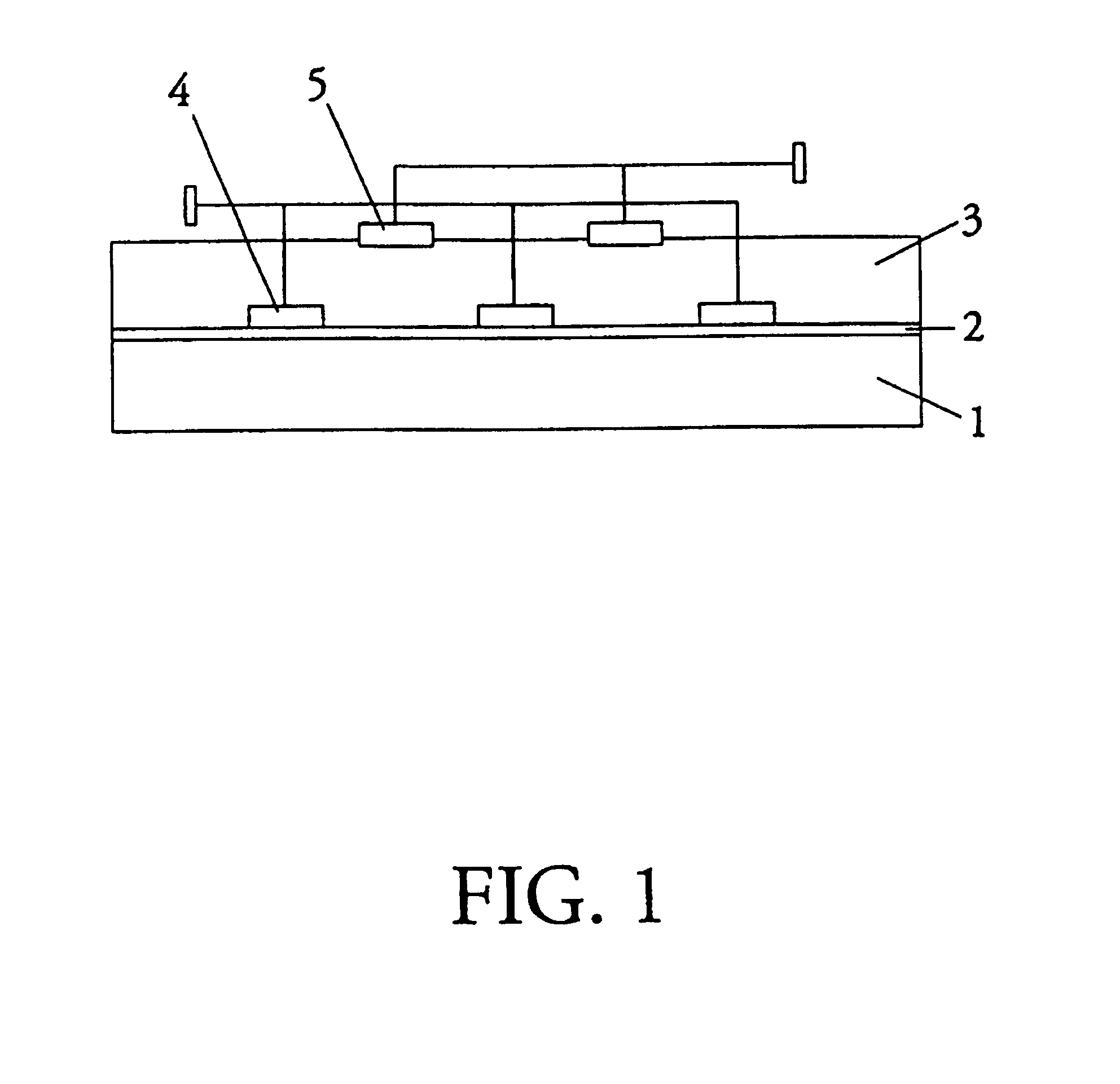
[0112]A carrier substrate 1 of glass is provided with a barrier layer 2 of TiO2. A lower interdigitated electrode 4 of Ti / Pt is provided on this barrier layer 2. A dielectric 3 of BaTiO3 is disposed over the lower interdigitated electrode 4. An upper interdigitated electrode 5 of Pt is provided on said dielectric 3.

embodiment 2

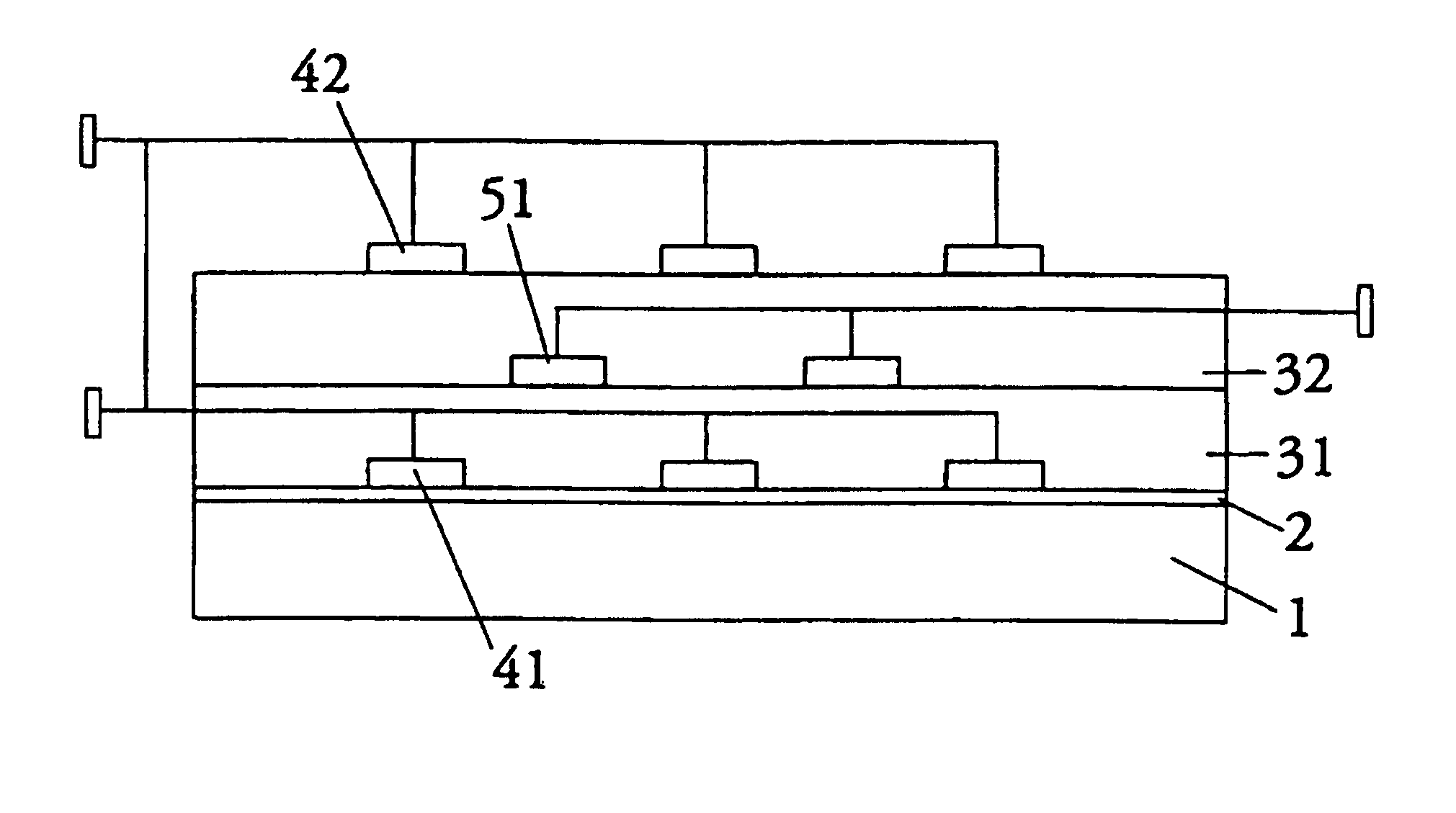
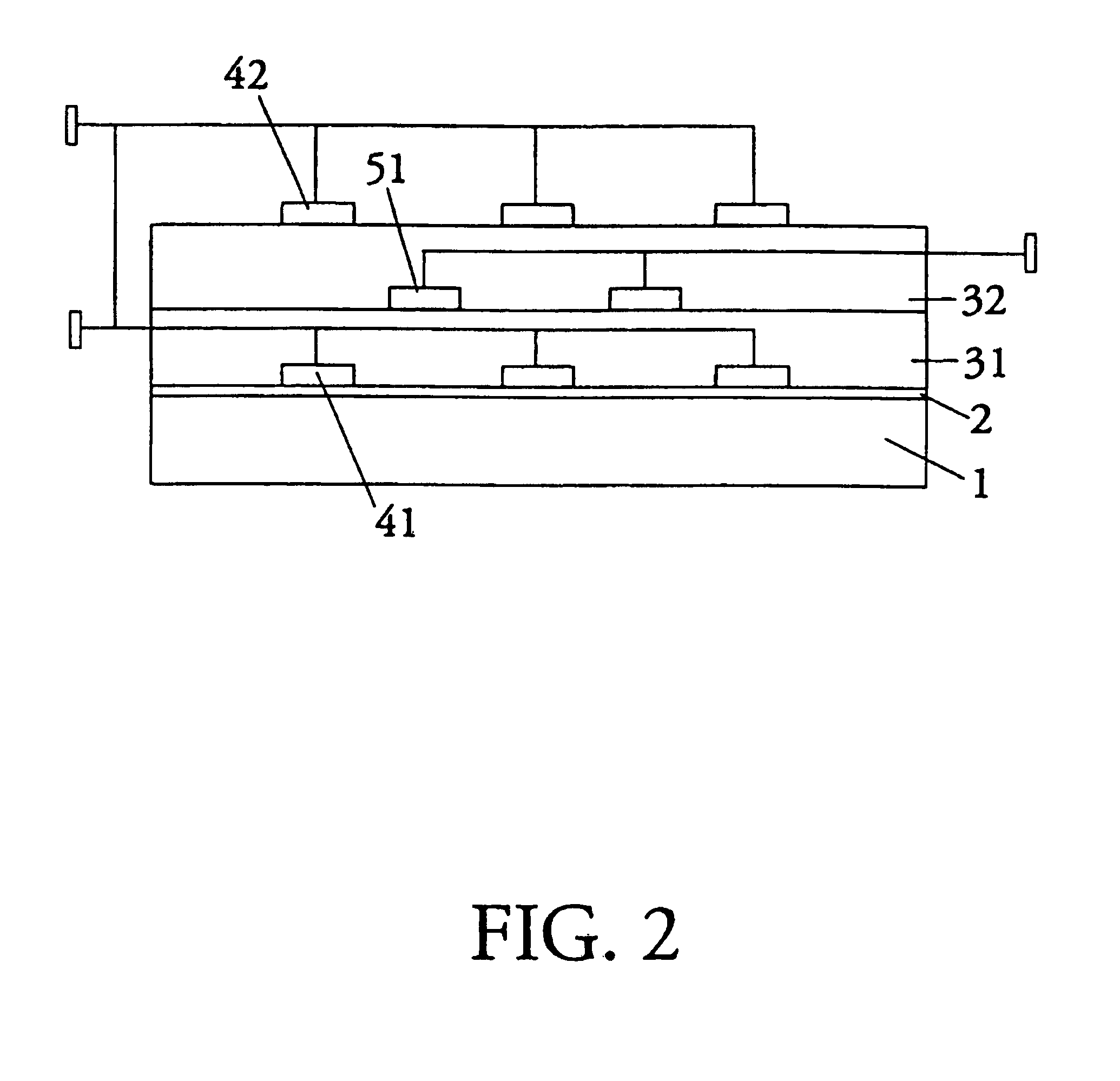
[0113]A carrier substrate 1 of glass is provided with a barrier layer 2 of TiO2. A lower interdigitated electrode 4 of Ti / Pt is provided on this barrier layer 2. A dielectric 3 of Pb(Zr0.53T0.47)O3 doped with lanthanum is disposed over the lower interdigitated electrode 4. An upper interdigitated electrode 5 of Pt is provided on said dielectric 3.

[0114]Standard monolayer capacitors are also manufactured in the same manufacturing process. The results of three tests are summarized in Table 1 below.

[0115]

TABLE 1Standard Monolayer Capacitor with 20 V / μm and 13 nF / mm2Test 1Test 2Test 3AverageRel. Dielectric Constant1120106010701083εrDielectric [μm]0.7540.7840.7020.747Op. Voltage Urated [V]15

[0116]

TABLE 2Parameters for the interdigitated electrodesNumber of Fingers:12Number of Gaps:11Length of Finger Overlap [μm]:850Total Overlap Length [μm]:9350

Table 3 shows the average capacitance values C and the operating voltages Urated for thin film capacitors with interdigitated electrodes (paramet...


PUM


Abstract

The invention relates to a thin film capacitor with a carrier substrate, at least two interdigitated electrodes, and a dielectric. A staggered arrangement of at least one interdigitated electrode below the dielectric with respect to an interdigitated electrode above the dielectric results in a breakdown-resistant thin film capacitor which can be manufactured in the same production process as a standard monolayer capacitor.

Description

BACKGROUND OF THE INVENTION[0001]The invention relates to a thin film capacitor which comprises a carrier substrate, at least two interdigitated electrodes, and at least one dielectric.[0002]Dielectric materials with high dielectric constant values (εr>50) are used for achieving high capacitance values in capacitors of small dimensions. Dielectrics with εr>50 at dielectric thicknesses of 50 nm to 2 μm are made by means of thin film processes in the manufacture of of thin film capacitors. An inexpensive method which is used for depositing thin layers with εr>50 is a wet chemical thin film method such as, for example, the sol-gel method. The lower electrode in a thin film capacitor is made of a non-noble metal such as, for example, aluminum or copper, or a noble metal, for example silver, a silver alloy, or platinum. For the upper electrode, noble metals such as, for example, platinum, silver, silver alloys, or NiCr / gold are used, as for the lower electrode, or alternatively ...

Claims


Application Information

Patent Timeline
IPC IPC(8): H01G4/005H01G4/33H01L21/02
CPCH01L28/40H01L28/55H01L28/60
Inventor KLEE, MAREIKEHERRMANN, WILHELMMACKENS, UWEKEIZER, PAULUS H. M.
Owner NXP BV
Why Eureka
Try Eureka