[0018]The present invention has been made in view of the above-described points of problem and has an object to provide a highly reliable non-volatile
semiconductor memory device which solves the above-described points of problem and which realizes executing high-speed
programming and erasure by using a NAND type memory cell unit that suits high degree of integration.
[0020]According to the first characterizing constructional feature of the non-volatile
semiconductor memory device, if turning off the transistor composing the memory cell and applying a prescribed level of
voltage to both ends of the memory cell, in the reading operation it is possible to reading data that has been stored using the variable
resistive element as a storing carrier by discriminating the change in the reading current that corresponds to the resistance values of the variable resistive element. Also, by turning on the transistor, the
electric current that flows through that transistor becomes overwhelming. Therefore, this corresponding memory cell can be brought to an unselected state in which it is not a reading object. As a result of this, it can be made distinct from the selected memory cell in which the transistor is kept “off”. Further, in the
programming or erasing operation as well, with respect to the memory cell that is a programmed / erased object, the transistor composing that memory cell is turned off. In this condition, there is adjusted the value, or polarity, of the voltage that is applied to both ends of the memory cell as in the case of the reading operation. By doing so, it is possible to vary the resistance value of the variable resistive element and therefore it becomes possible to execute storing (program / erasure) of data using the variable resistive element as a storing carrier. Also, regarding the unselected memory cell as well, by turning on the transistor of the unselected memory cell as in the case of the reading operation, the program or erasure voltage that is to be applied to both ends of the variable resistive element becomes stopped from being applied by the transistor that is kept on. Therefore, storing (
programming or erasing) the data can be selectively prohibited. That is to say, it is possible to provide a semiconductor memory device which, by selecting as the variable resistive element the material that enables appropriately adjusting the amplitude and width of a
pulse voltage applied to both ends of the memory cell and enables high-speed program and erasure, enables realizing high-speed program and erasure and eliminates the necessity of causing a flowing of a large current when executing program and erasure and which, as a result, has a high level of reliability.
[0021]Also, by adopting a memory
cell structure wherein a transistor and variable resistive element formed on the semiconductor substrate are connected in parallel and by adopting as the variable resistive element the one having the characteristic that its resistance value varies by applying a voltage with respect to it, since between at the time of reading and at the time of programming the selected / unselected operations for the memory cells are the same in terms of the logical construction, simplifying the
peripheral circuits such as a decoder circuit, etc. can also be achieved.
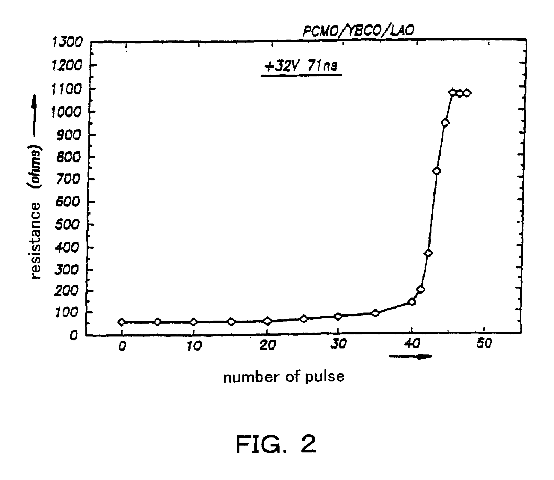
[0023]According to the second characterizing constructional feature of the non-volatile semiconductor memory device, it is possible to realize a variable resistive element that enables obtaining a change in resistance that occurs to an extent of one place or two or more places by adjusting the amplitude and width of a
pulse voltage applied to both ends of the memory cell, for example, by applying a programming
pulse voltage with a
voltage amplitude of not more than 7V and with a pulse width of not more than 100 ns and with respect to that, therefore, high-speed and low-power program and erasure can be performed, and it is possible to provide a non-volatile semiconductor memory device which, as a result of that, enables executing high-speed program and erasure.
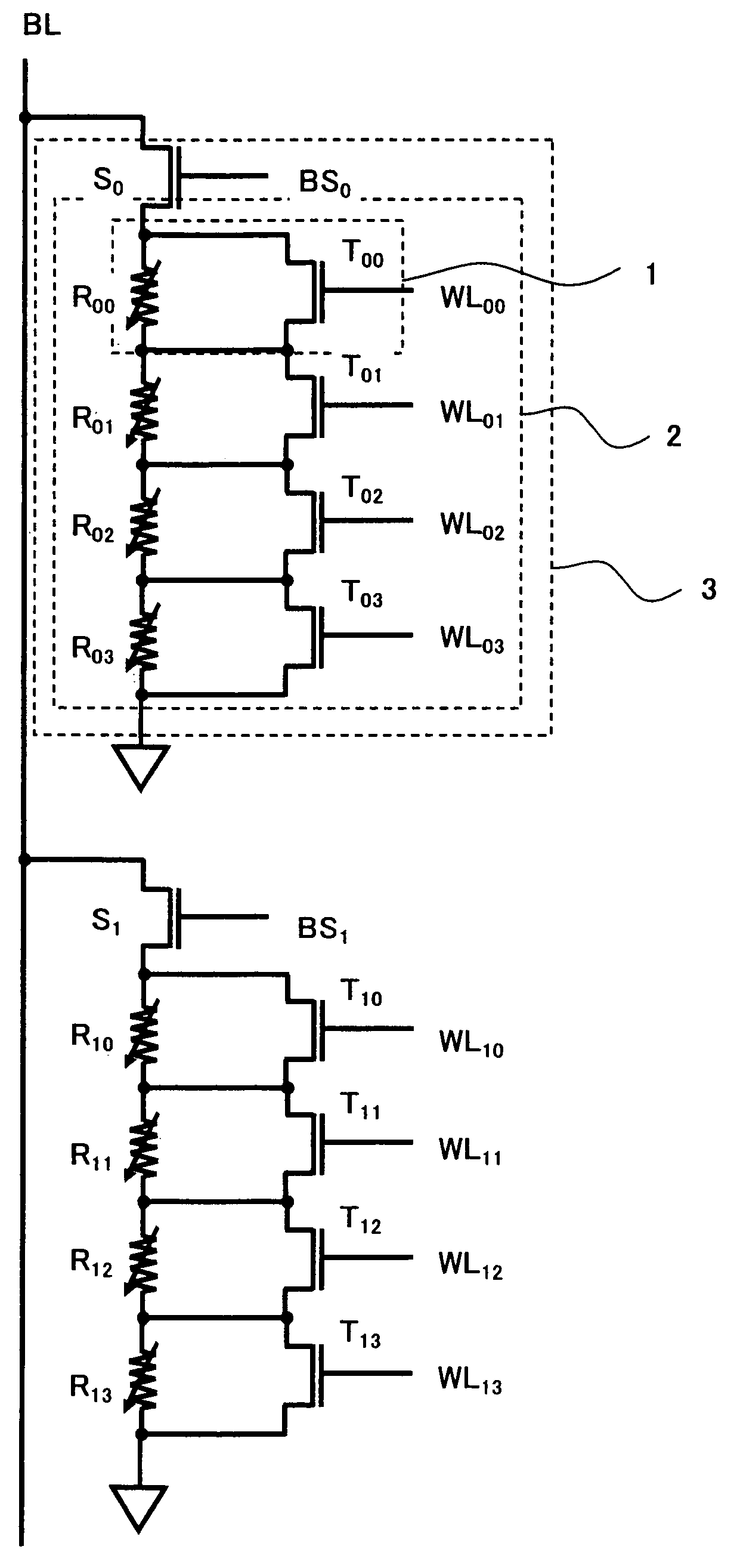
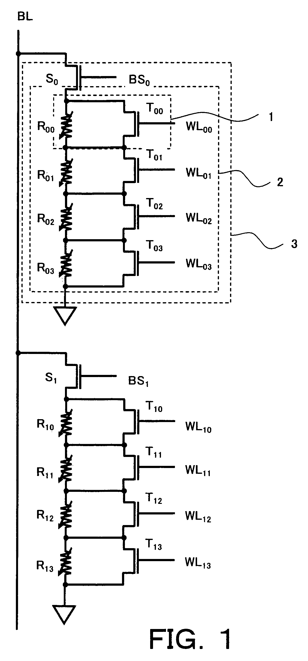
[0025]According to the third and fourth characterizing constructional features of the non-volatile semiconductor memory device, the device is made up into a so-called NAND type cell array structure wherein the memory size per bit can greatly be reduced and it is therefore possible to provide a non-volatile semiconductor memory device with respect to which high-speed program and erasure are possible and which therefore has a high level of reliability. Especially, according to the above-described fourth characterizing feature, by connecting in parallel a plurality of the memory cell blocks and connecting one end of each memory
cell block to a
bit line for applying a reading or programming / erasing voltage, the capacity of the device can be enlarged while limiting the number of memory cells in the memory cell connected-in-series part, namely preventing the great decrease in the reading speed.
[0027]According to the above-described fifth characterizing constructional feature of the non-volatile semiconductor memory device according to the present invention, in a case where having applied a prescribed level of reading, programming, or erasing voltage to both ends of the relevant memory cell connected-in-series part, it is possible to suppress to a small value the
voltage drop in the memory cell that is kept in a unselected state and it is thereby possible to highly efficiently apply a necessary voltage to both ends of the memory cell that has been selected. Namely, it is possible to make great the change in the
electric current flowing through the selected memory cell correspondingly to the status of resistance value of the variable resistive element in the selected memory cell. This enables increasing the reading speed and making large the margin for operation. Also, since the level of the voltage that is applied to both ends of the unselected memory cell can be lowered, it is possible to suppress the program-disturbing phenomenon that when programming of data is performed the data in the unselected memory cell is destroyed.

