Switching matrix configuration for reducing loss

a switching matrix and loss reduction technology, applied in the direction of optical elements, instruments, optical waveguide light guides, etc., can solve the problems of reducing reducing the design limitation of optical transmission through switching systems, and increasing the complexity of system configurations, so as to reduce the size and cost of optical switches, simplify the production of large-scale optical switches, and enhance the strength of gratings

Inactive Publication Date: 2006-02-21
INTERGRATED OPTICS COMM
View PDF7 Cites 8 Cited by
  • Summary
  • Abstract
  • Description
  • Claims
  • Application Information

AI Technical Summary

Benefits of technology

[0014]Electrostatic bending of a waveguide with integrated Bragg grating can be implemented by simply applying a voltage between a silicon substrate and an electrode. This can greatly simplify the production of large-scale optical switches, comparing with the micro-mirror based MEMS approach.
[0015]The integrated Bragg grating is formed by physically corrugating a waveguide. Thus, it does not reply upon a photorefractive index change, which enables building Bragg gratings in material that are not photo-refractive and enhancing the grating strength. The integrated Bragg grating can be made smaller, and packed closer together than fiber-optic device. This opens the door for leveraging IC processing to fabricate the highly integrated optical switches.
[0016]In accordance with the invention, the switch matrix constructed by the method as that disclosed in this invention performs the de-multiplexing and re-multiplexing functions inherently. Therefore, in a preferred embodiment, no external de-multiplexers and complicated re-multiplexers are needed to form an optical switching functional block. The size and cost of the optical switches are significantly reduced according to the disclosures made in this invention.

Problems solved by technology

Current state of the art in optical switching and signal transmission system is facing with at least two limitations that 1) an optical signal switching operation is performed without wavelength selectivity, and 2) even in a wavelength selective matrix switching system the losses in optical transmission through a switching system become a significant design limitation particularly for larger switching matrix systems.
This requirement leads to more complicate system configurations, higher manufacture and maintenance costs, and lower system reliability.
However, with the current technical limitations, an all fiber network implemented with optical switches are still quite expensive.
On the other hand, these products and their methods of use are disadvantageous in the following aspects: first, in these switches, light travels through free space, which causes unbalanced power loss.
Secondly, in order to steer each mirror, three to four electrodes need to be connected to each mirror, which is a major challenge to produce large-scale mechanical-type MEMS-based switches.
Thirdly, alignment and packaging are difficult tasks particularly for large-scale switches.
The disadvantages of these devices are their reliability issues and the insertion loss issue for the large-scale switches.
A common drawback of both of these two types of MEMS-based switches is the requirement to work with external de-multiplexing and re-multiplexing systems in order to function properly in an optical networking system.
The requirements of implementing de-multiplexing and re-multiplexing functions add tremendous complexities to the system configuration and significantly increase the cost of manufacture, system installation, and maintenance of the optical network systems.
Another drawback of both of these two types of MEMS-based switches is that these prior art switching systems are not wavelength selective switches.
In another word, the switching systems cannot selectively switch a particular wavelength from an input waveguide to a desired output waveguide.
In short, they are not wavelength intelligent devices.
To date, this new, promising Bragg grating technology has not been deployed to build up a system implemented with wavelength intelligent optical switches.

Method used


Image

  • Switching matrix configuration for reducing loss
  • Switching matrix configuration for reducing loss
  • Switching matrix configuration for reducing loss

Examples


Embodiment Construction

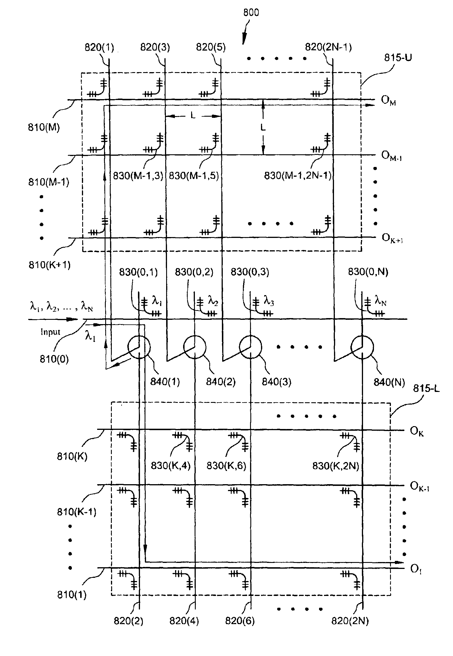
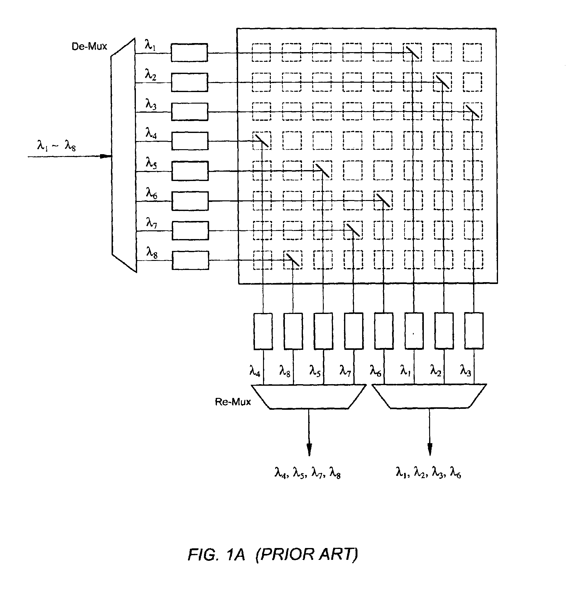
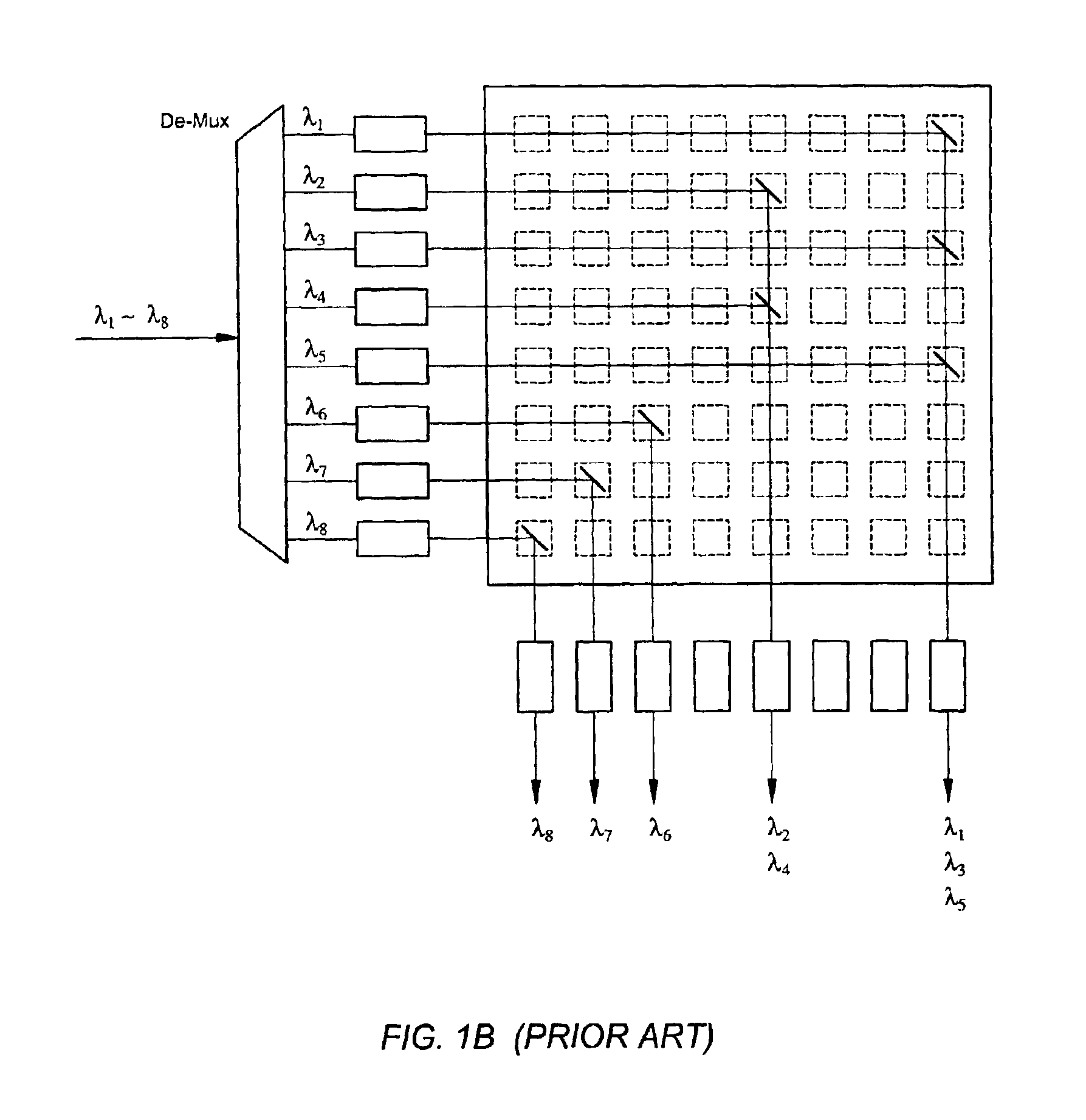
[0025]FIGS. 2A and 2B are schematic diagrams for showing the on and off states respectively of a wavelength-selective bridge waveguide 120 relative to a multi-channel bus waveguide 110. A multiplexed optical signal is transmitted in a bus waveguide 110 over N multiplexed wavelengths λ1, λ2, λ3, . . . λN where N is a positive integer. In FIG. 2A, the wavelength selective bridge waveguide 120 is moved to an on-position and coupling to the waveguide 110. An optical signal with a central wavelength λi particular to the Bragg gratings 125 disposed on the bridge waveguide 120 is guided into the wavelength selective bridge waveguide 120. The remainder optical signal of the wavelengths λ1, λ2, . . . , λi−1, λi+1, . . . , λN is not affected and continues to transmit over the waveguide 110. The Bragg gratings 125 have a specific pitch for reflecting the optical signal of the selected wavelength λi onto the wavelength selective bridge waveguide. In FIG. 2B, the wavelength selective bridge wave...


PUM


Abstract

The present invention discloses a switching matrix configuration to reduce the optical propagation losses and coupling losses. The switching matrix comprises M horizontal waveguides interested with 2N vertical waveguides, where M and N are positive integers and the optical switching system is configured to receive a multiplexed input optical signal from a horizontal waveguide disposed next to an i-th horizontal waveguide where i is a closest integer to a positive real number M/2.

Description

[0001]This application claims priority to pending U.S. provisional patent application entitled WAVEGUIDE GRATING-BASED WAVELENGTH SELECTIVE SWITCH ACTUATED BY MICRO-ELECTROMECHANICAL SYSTEM filed Oct. 22, 2001 by Zhang et al. and accorded Ser. No. 60 / 348,927, the benefit of its filing date being hereby claimed under Title 35 of the United States Code.BACKGROUND OF THE INVENTION[0002]1. Field of the Invention[0003]This invention relates generally to technologies for switching and routing optical wavelengths. More particularly, this invention relates to switching matrix configuration for reducing optical transmission losses in a grating-based wavelength selective switching matrix system.[0004]2. Description of the Related Art:[0005]Current state of the art in optical switching and signal transmission system is facing with at least two limitations that 1) an optical signal switching operation is performed without wavelength selectivity, and 2) even in a wavelength selective matrix swit...

Claims


Application Information

Patent Timeline
Patent Type & Authority Patents(United States)
IPC IPC(8): G02B6/35G02B6/293G02B6/34G02B6/12G02B6/124G02B6/28H04Q11/00
CPCG02B6/124G02B6/29319G02B6/3508H04Q11/0005G02B6/2852G02B6/3536H04Q2011/0049G02B6/356G02B6/3596G02B2006/12107G02B6/3546
Inventor ZHANG, JIANJUNLING, PEICHINGCHEN, JINLIANGXU, MING
Owner INTERGRATED OPTICS COMM
Why Eureka
Try Eureka