Device for probe card power bus noise reduction

a power bus and power supply technology, applied in the field of electronic circuit testing, can solve the problems of inability to fully compensate the noise spike, the noise pulse the noise spike produced by the sequence, so as to reduce the power supply spike of the probe card and improve the regulation of the voltage bus

Inactive Publication Date: 2006-02-28
GLOBALFOUNDRIES INC
View PDF4 Cites 130 Cited by
  • Summary
  • Abstract
  • Description
  • Claims
  • Application Information

AI Technical Summary

Benefits of technology

[0011]This invention addresses the problem of reducing probe card power supply spikes in the intermediate range, from 1 ns to 10 μs time scale range where the traditional probe card capacitor bypass network solution is becoming ineffective. The device according to the present invention addresses this problem by using active regulation circuitry mounted directly on the probe card. This approach leads to a large improvement in the regulation of the voltage bus over a conventional passive capacitor bypass of the same net capacitance value.

Problems solved by technology

When the DUT contains a large number of transistors, this test sequence invariably produces a voltage noise pulse on the power planes of the probe card used to bias the DUT.
The noise spike is produced by momentary increase in current drawn by the chip during the test cycle.
This noise spike cannot be fully compensated by the on chip decoupling capacitor network.
These voltage noise spikes (which momentarily reduce the power supply voltage applied to the DUT) can cause the DUT to fail the applied test pattern if the voltage reduction is severe enough, event though the DUT is defect free.
It should be pointed out that, because of the transient nature of structural test patterns, it is impossible to eliminate these voltage noise spikes by the application of conditioning cycles prior to the test.
However, as the current requirements of the DUT have increased, and voltage levels have decreased, even these longer time voltage transients have become more difficult to tame, because they have become larger in amplitude.
However, even with the best POL power supply electronics, practical considerations (the regulation units are physically large and hence cannot be located on the probe card, the probe card / power supply interface contains significant inductive parasitics, etc.) make the fastest response times of these units 5 microseconds or greater.
However, as the level of integration of silicon circuits has increased, voltage supply levels have decreased and current requirements have increased.
Increasing DUT supply current requirements in combination with a fixed probe card area for the mounting of decoupling capacitors is making it impossible to provide enough bypass capacitance to adequately reduce voltage noise spikes in the 1 ns to 10 μs time range when testing state of the art components with very high supply currents (˜100 amps).
Adding more capacitance farther away from the DUT is not effective for reducing high frequency noise spikes because the time constant of the bypass network becomes too great.
The size of capacitors is limited too; using capacitors with larger capacitance values in the same area is ineffective if the larger capacitors have larger Equivalent Series Inductance (ESL) or Equivalent Series Resistance (ESR) values.
Although many different technologies are available for capacitors, one rule generally holds true: as technologies are employed with a higher capacitance to volume ratio (specific capacitance), ESL and ESR increase, making them less effective at filtering the higher frequency voltage spikes.
This restricts the capacitors used to filter transients in the Ins to 10 μs range to high performance, low ESR and ESL types with low specific capacitance values, which limits the total capacitance of the network because of the limited space available on the probe card close to the DUT.

Method used


Image

  • Device for probe card power bus noise reduction
  • Device for probe card power bus noise reduction
  • Device for probe card power bus noise reduction

Examples


Embodiment Construction

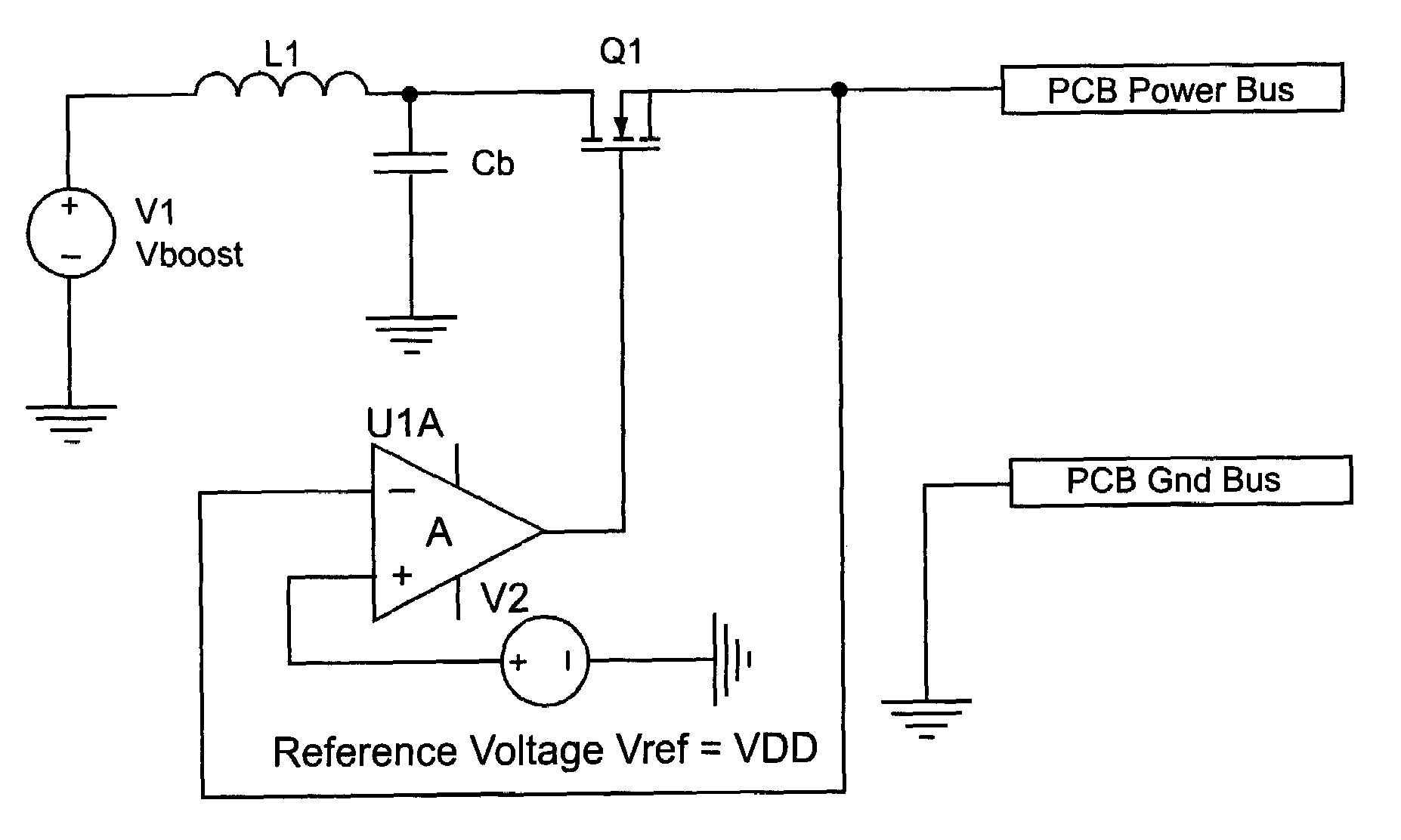
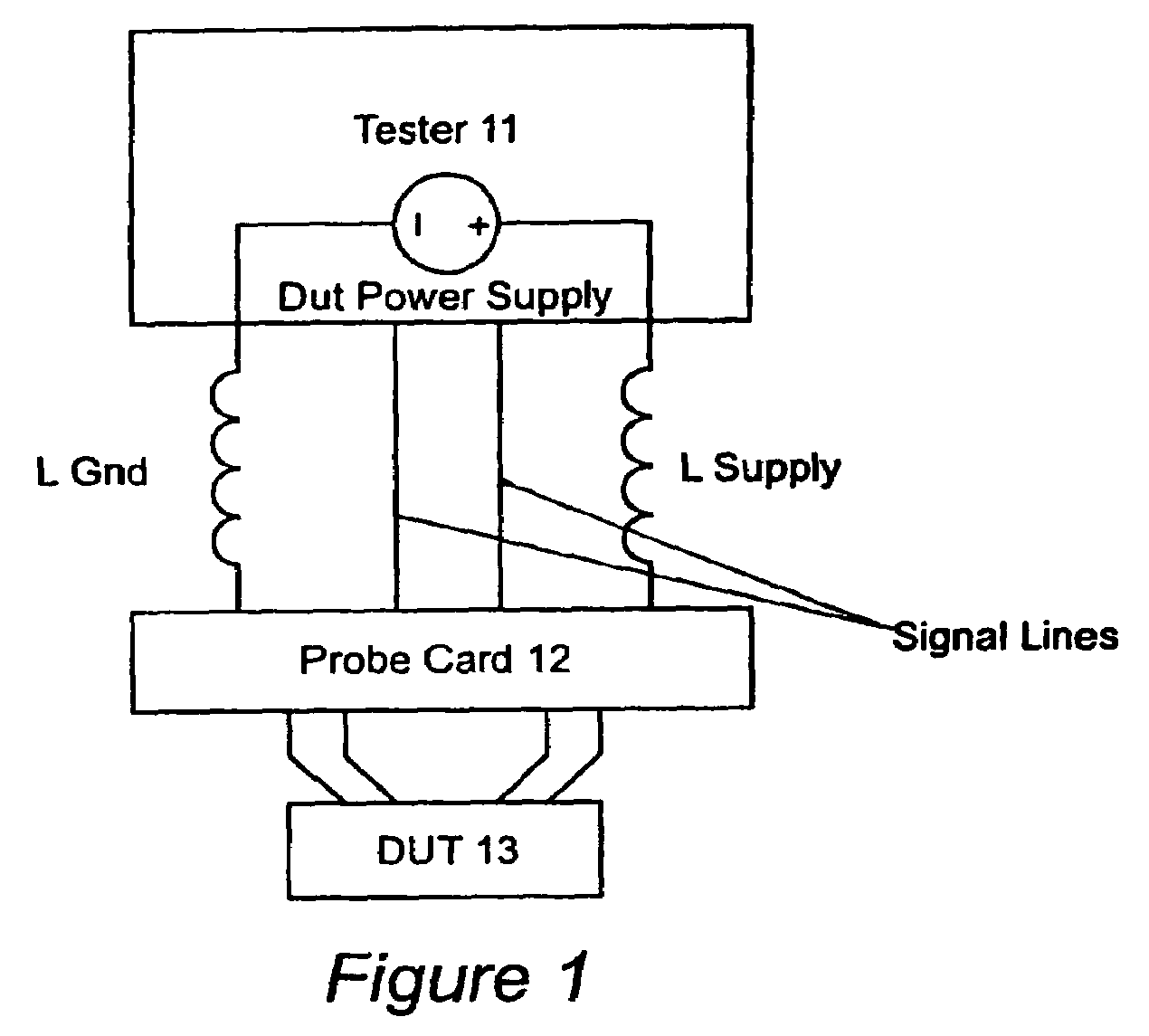
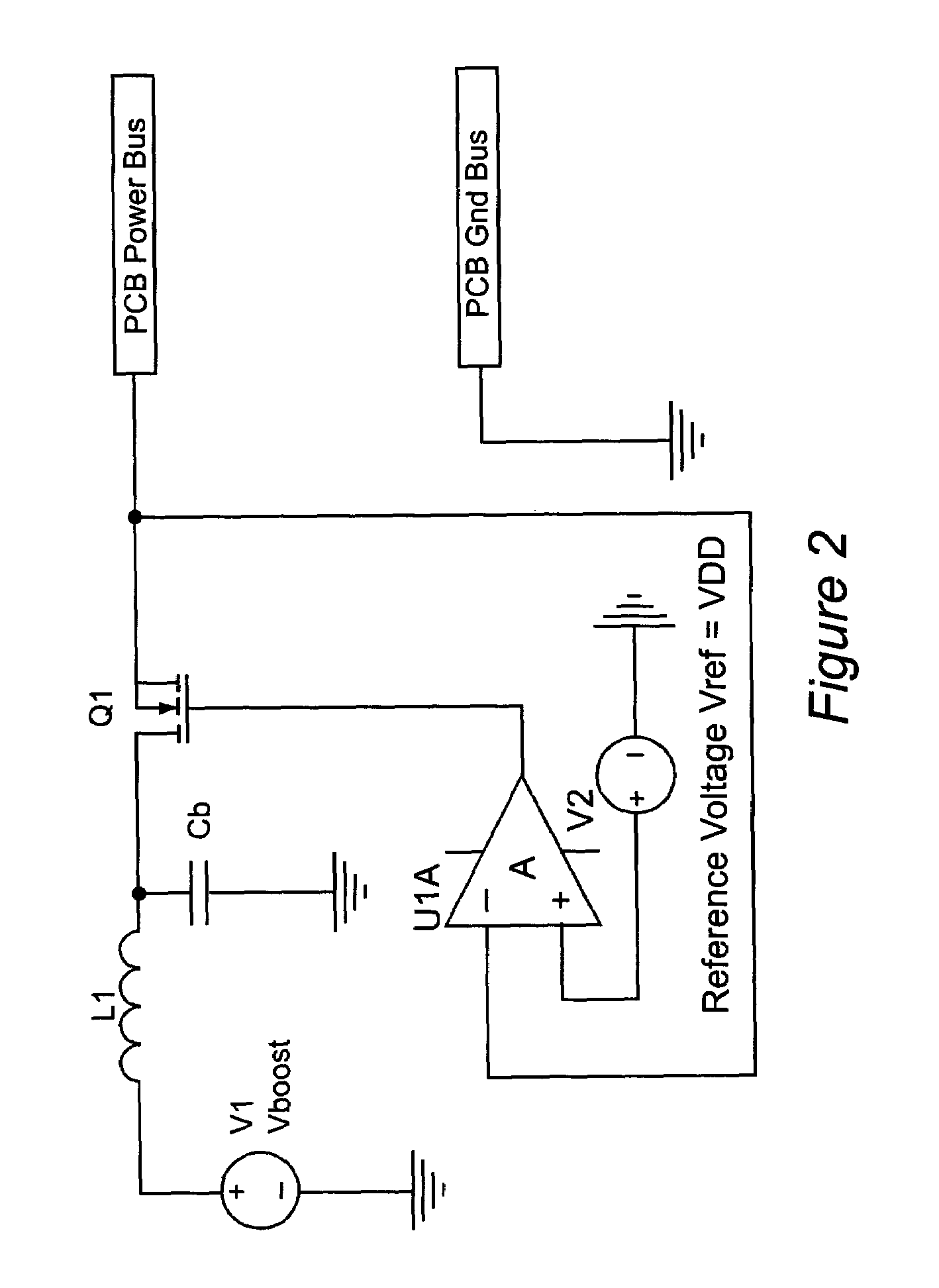
[0021]Referring now to the drawings, and more particularly to FIG. 1, there is shown a system for testing integrated circuits. In its most basic form, the system consists of a tester 11, probe card 12, and integrated circuit 13, or DUT. The tester provides both power and stimulus to the DUT. The probe card provides the interface between the tester and DUT, and includes a power distribution system, which often includes passive elements mounted on the probe card (capacitors) to control the size of power system noise spikes caused by the DUT during operation. Also indicated in FIG. 1 is the connection inductance that the interface introduces between the tester power supply and the probe card. When the DUT supply current changes, this connection inductance (L Supply and L GND) can cause significant voltage noise spikes to appear across the power bus system of the probe card. One source of change in the DUT supply current is the application of structural test patterns to the DUT. In a st...


PUM


Abstract

Noise reduction for application of structural test patterns to a Device Under Test (DUT) is accomplished with a capacitor “booster” bypass network on the probe card in which the capacitors are charged to a much higher voltage Vboost than the DUT power supply voltage VDD. Charging the capacitors to a voltage N×VDD allows the buster network to store N times the charge of a conventionally configured capacitance network, and effectively provides N times the capacitance of the original network in the same physical space.

Description

BACKGROUND OF THE INVENTION[0001]1. Field of the Invention[0002]The present invention generally relates to electronic test circuits and, more particularly, to testing microelectronics at wafer level.[0003]2. Background Description[0004]The test of state of the art microelectronics at wafer level often requires the application of structural test patterns to the Device Under Test (DUT). In a structural test, the DUT is loaded with an input pattern of test vectors, a single clock cycle is applied, and the resultant output vector is read out. Often this test sequence is repeated many times during the course of the test, in rapid succession. When the DUT contains a large number of transistors, this test sequence invariably produces a voltage noise pulse on the power planes of the probe card used to bias the DUT. The noise spike is produced by momentary increase in current drawn by the chip during the test cycle. This noise spike cannot be fully compensated by the on chip decoupling capac...

Claims


Application Information

Patent Timeline
Patent Type & Authority Patents(United States)
IPC IPC(8): G01R31/26
CPCG01R31/2879G01R31/31723G01R31/31721
Inventor ROBERTAZZI, RAPHAEL PETER
Owner GLOBALFOUNDRIES INC
Why Eureka
Try Eureka