Mask ROM fabrication method

Inactive Publication Date: 2006-03-07
SAMSUNG ELECTRONICS CO LTD
View PDF12 Cites 2 Cited by
  • Summary
  • Abstract
  • Description
  • Claims
  • Application Information

AI Technical Summary

Benefits of technology

[0041]Therefore, according to the present invention, the area of the cell array region can be effectively reduced, and a parasitic capacitance between the word lines and the semiconductor substrate, the sheet resistance of the buried impurity diffusion regions, and the parasitic junction capacitance between the semiconductor substrate and the buried impurity diffusion regions, can all be reduced.

Problems solved by technology

However, if the size of a semiconductor device is reduced by the above-mentioned method, investment costs for equipment capable of producing a new generation semiconductor device increase logarithmically.
Such a high-cost investment in the high integration of semiconductor devices becomes a burden to a manufacturer.
As the design rule decreases for highly integrated devices, the size of a bar “B” of the photoresist pattern 38 (which determines the length of the channel regions)may decrease to be less than a desired size, as a result of various limitations in the photolithography technology.
Thus, the marginal size of bar “B” may hinder the reduction of cell size.

Method used


Image

  • Mask ROM fabrication method
  • Mask ROM fabrication method
  • Mask ROM fabrication method

Examples


first preferred embodiment

[0052]FIG. 9 is a plan view of a cell array region of a NOR type mask ROM according to preferred embodiments of the present invention, and FIGS. 10 through 13 are sectional views taken along lines X–X′, XI–XI′, XII–XII′ and XIII–XIII′ of FIG. 9, respectively.

[0053]FIGS. 9 through 13, reference numeral 70 represents a semiconductor substrate, reference numeral 72 represents a buried impurity diffusion region, reference numeral 74 represents a gate insulation layer, reference numeral 76 represents a grown insulation layer, reference numeral 78 represents a pad conductive layer, reference numeral 80 represents a word line (i.e., a gate), reference numeral 82 represents a gate protective insulation layer, reference numeral 84 represents a planarization layer, reference numeral 86 represents a metal interconnection, reference numeral 88 represents a metal interconnection protective insulation layer, reference numeral 89 represents a channel region of a cell, which requires programming an...

second preferred embodiment

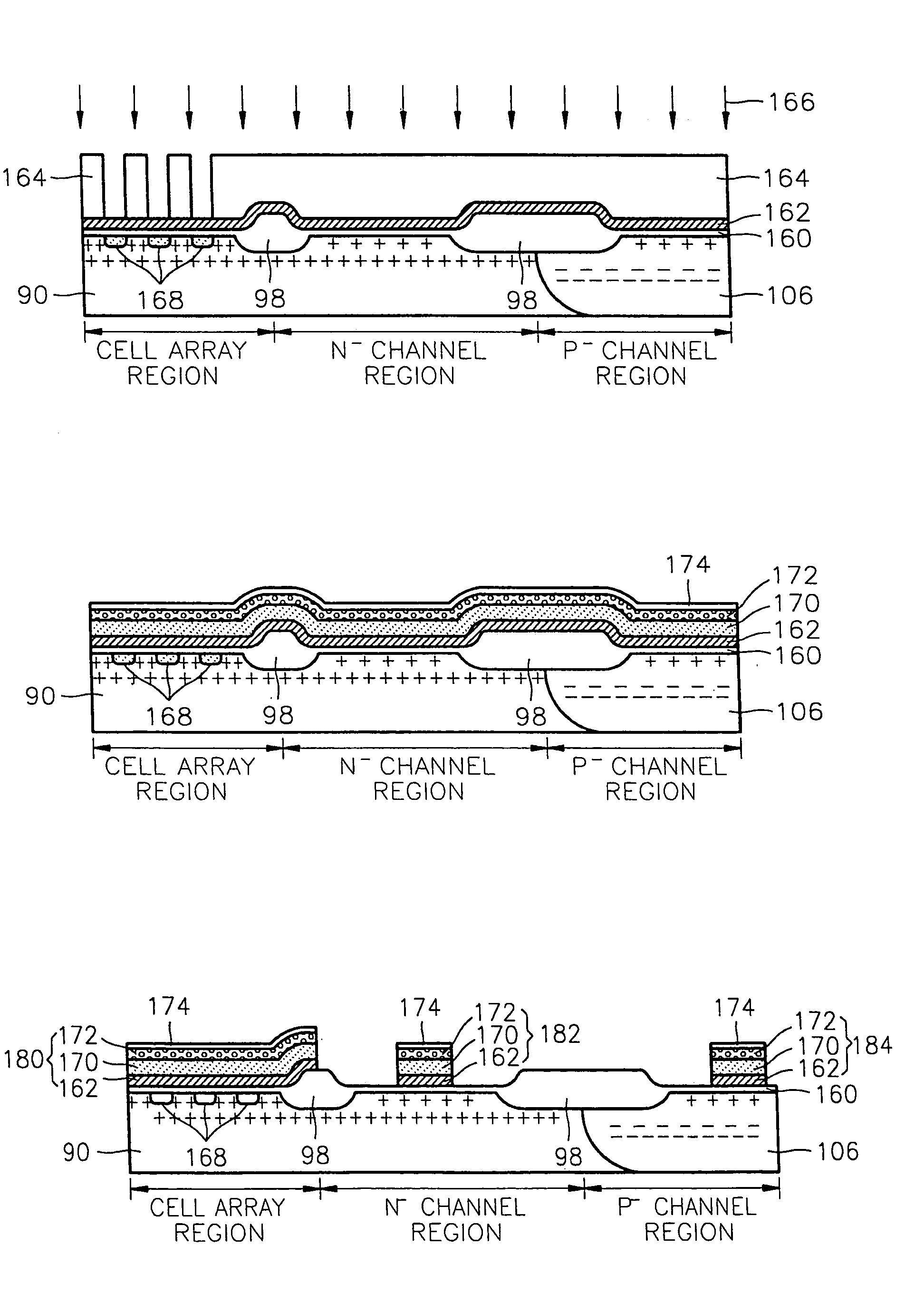
[0088]FIGS. 22 through 25 are sectional views illustrating a method of fabricating a mask ROM having buried impurity diffusion regions according to a second preferred embodiment of the present invention, and in particular, illustrating in greater detail the formation of the pad conductive layer patterns and the grown insulation layer. In the present embodiment, the etching process for the conductive layer pattern is performed after the formation of spacers, rather than immediately after the formation of a first etch mask layer.

[0089]First, referring to FIG. 22, a conductive material layer 114 for a pad conductive layer is formed over a gate insulation layer 112 formed on a semiconductor substrate 90, and a first etch mask layer 116 is formed on the conductive material layer 114. The thickness of each layer is the same as that illustrated in the first preferred embodiment. During the formation of the first etch mask layer 116, the thickness of the remaining conductive material layer ...

third preferred embodiment

[0094]In the second preferred embodiment, word lines, which act as the gate electrodes of cell transistors, are formed in a structure where polycide layers, i.e., the first polysilicon layer, a second polysilicon layer, and a metal silicide layer, are sequentially stacked. Unlike in the first preferred embodiment where the conductive layers are formed as patterns (i.e., the pad conductive layers 114c) in the channel regions of cells, the first polysilicon layer of the second preferred embodiment is arranged extending in the same direction with the same pattern as that of the word lines. Here, the first polysilicon layer is preferably formed to a thickness of, e.g., 100–1000 Å, which is thick enough to act as an anti-reflective layer (ARL).

[0095]FIGS. 26 through 28 are sectional views sequentially illustrating a method of fabricating a mask ROM having buried impurity diffusion regions according to the second preferred embodiment of the present invention. First, referring to FIG. 26, ...


PUM


Abstract

A mask read only memory (ROM) and a method of fabricating the same is provided. This mask ROM and related method is capable of reducing the pitch of buried impurity diffusion regions. In the mask ROM fabrication process, a gate insulation layer is formed over a semiconductor substrate, and parallel conductive layer patterns are formed on the gate insulation layer. These conductive layer patterns are separated from each other by a first predetermined interval and extend in the same direction. Ion implantation is then carried out using the conductive layer patterns as a mask to form buried impurity diffusion regions near the semiconductor substrate between the conductive layer patterns. A conductive layer for use in forming word lines is then formed over the entire surface of the resultant structure, and both the conductive layer and the conductive layer patterns are etched so as to form word lines and pad conductive layers. The word lines are formed to be parallel to each other, are separated from each other by a second predetermined interval, and extend in a direction perpendicular to the buried impurity diffusion regions. The pad conductive layers, which form ohmic contacts with the word lines, are formed in an island shape channel regions. These channel regions are defined as the areas between the buried impurity diffusion regions that are overlapped by the word lines.

Description

CROSS REFERENCES TO RELATED APPLICATIONS[0001]This application is a divisional of U.S. patent application Ser. No. 09 / 566,916 filed on 9 May 2000 now abandoned and claims priority under 35 U.S.C. 119 to Korean Application No. 99-16605, filed on 10 May 1999, and upon Korean Patent Application No. 00-3398, filed 25 Jan. 2000, the contents of both of which are hereby incorporated by reference in its entirety for all purposes.BACKGROUND OF THE INVENTION[0002]The present invention relates to a method of fabricating a semiconductor device, and more particularly, to a method of fabricating a mask read only memory (ROM) capable of effectively reducing the distance between buried impurity diffusion regions.[0003]As the level of integration of semiconductor devices increases, the scaling-down of a pattern pitch, i.e., decreasing of the size of a line / space of a circuit, becomes an important consideration. Such a decrease in the size of a line / space of a circuit is achieved by developing photo...

Claims


Application Information

Patent Timeline
IPC IPC(8): H01L21/8236H01L27/112A61B5/055G01N24/00G01R33/20H01L21/8246
CPCH01L27/1126H01L27/112H10B20/383H10B20/00
Inventor LEE, WOON-KYUNGLEE, HE-JUENGKIM, EUI-DO
Owner SAMSUNG ELECTRONICS CO LTD
Why Eureka
Try Eureka