ESD protection devices and methods for reducing trigger voltage

a protection device and trigger voltage technology, applied in the direction of solid-state devices, resistors, basic electric elements, etc., can solve the problems of local heating, affecting the esd protection level, and becoming more vulnerable to the impact of external environment, so as to achieve a tighter trigger mechanism and improve the effect of esd protection level

Inactive Publication Date: 2006-03-07
WINBOND ELECTRONICS CORP
View PDF11 Cites 45 Cited by
  • Summary
  • Abstract
  • Description
  • Claims
  • Application Information

AI Technical Summary

Benefits of technology

[0017]The advantage of the MOS structure according to the present invention is that its ESD protection trigger voltage is lower by the existence of the island. It implies that the MOS structure has a quicker trigger mechanism and a better ESD protection level when compared to the case without the island.

Problems solved by technology

As products based on integrated circuitry (ICs) become more delicate, they also become more vulnerable to the impacts of external environment, especially to ESD stress occurring when one pin of an IC is grounded and anther pin of the IC contacts an electrostatically-precharged object.
If the ESD transient current starts to localize at a weak spot near the gate, it causes the entire ESD current to rush in, thereby causing local heating and eventually damaging the NMOS.
The advanced salicide process, which forms silicide material on drain / source regions to reduce the resistance of active regions and speeds up the circuit operation rate, however, makes construction of the above-mentioned resistor more difficult and costly.
However, this solution is inefficient due to the process complexity and the extra mask required.

Method used


Image

  • ESD protection devices and methods for reducing trigger voltage
  • ESD protection devices and methods for reducing trigger voltage
  • ESD protection devices and methods for reducing trigger voltage

Examples


first embodiment

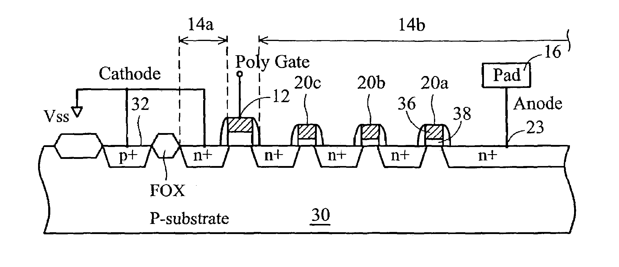
[0038]FIG. 2 shows a layout view of an NMOS structure according to the present invention. FIG. 3 is a cross-section of the NMOS structure in FIG. 2 along a portion of line A–A′.

[0039]The ESD protection device in FIG. 2 is a multi-finger-type NMOS with two poly gates 12 coupled together. The gate oxides of these two poly gates 12 are thick oxide gates. An active region 14 is surrounded by a field oxide (FOX) isolation region, which is typically formed by local oxidation (LOCOS) or shallow trench isolation (STI). The active region 14 is typically ion-implanted by negative-type ions and then annealed by thermal cycles to form heavily n-doped (n+) layers. The ion implant is blocked by any poly gate, poly segment or field oxide region present within the active region. Within the active region 14, two channel regions under the poly gates 12 are formed. The portion of the active region 14 between the two poly gates 12 is referred to as a drain diffusion region 14b, serving as an anode and ...

second embodiment

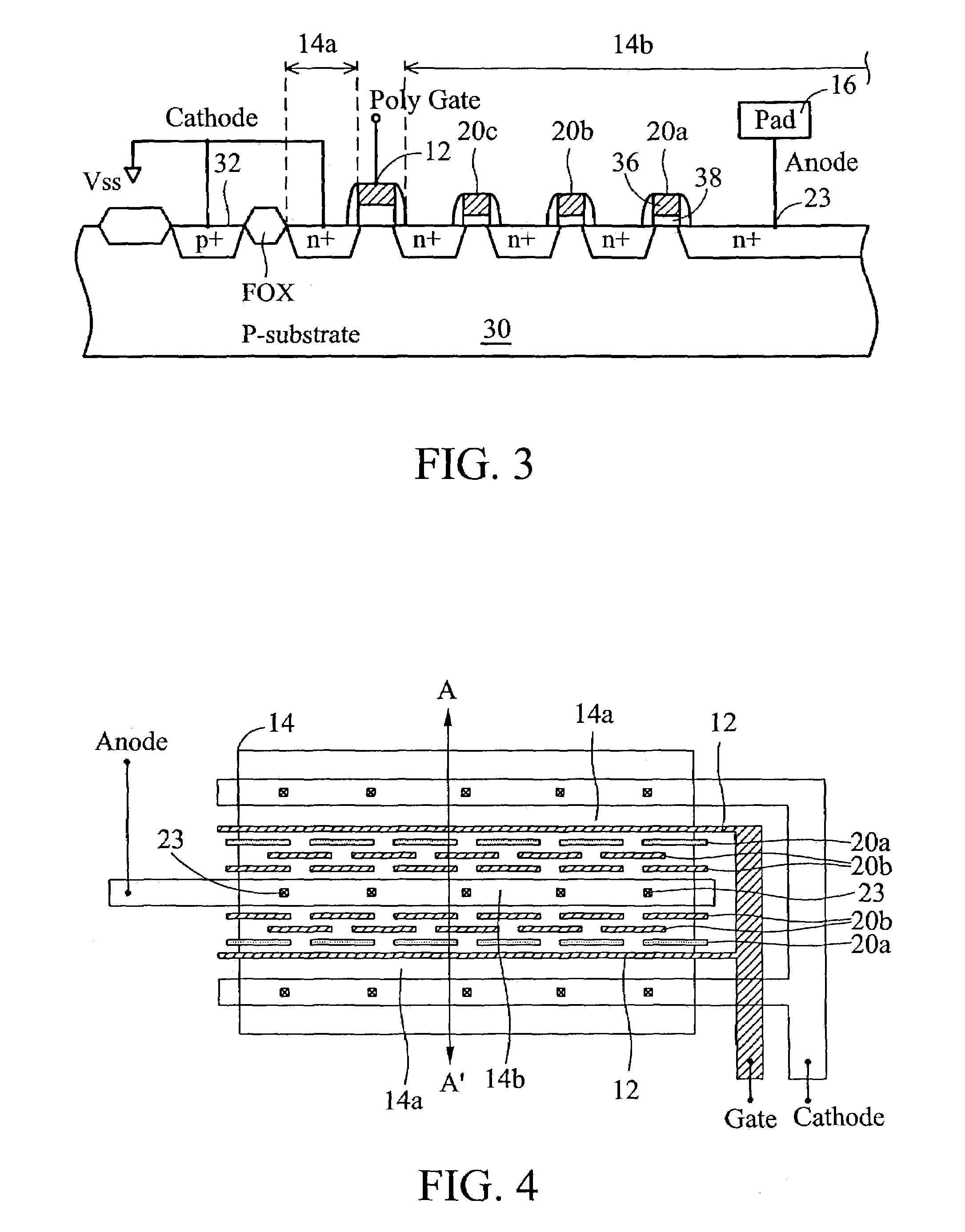
[0044]FIG. 4 shows a layout view of an NMOS structure with islands of different gate oxide thickness according to the present invention. FIG. 5 is a cross-section of the NMOS structure in FIG. 4 along a portion of line A–A′.

[0045]Not all the islands in the ESD protection device need thin gate oxides. Islands with thin gate oxides have two purposes: one is quicker triggering of the NMOS to discharge ESD current, and the other is dispersing the current flow in the drain diffusion region 14b. The former purpose can be achieved even though there is only one island with a thin gate oxide overlaying the drain diffusion region. The latter purpose can also be achieved even when all the islands have thick gate oxides. Thus, the islands in the drain diffusion region 14b can have different gate oxides. FIGS. 4 and 5 depict this concept, where the islands 20a in the rows nearest the control gates have thin gate oxides for quicker triggering and the other islands 20b have thick gate oxides only ...

third embodiment

[0046]FIG. 6 shows a layout view of a field device ESD protection structure with strips of field gate oxides over channels between adjacent anode-coupled and cathode-coupled diffusion regions according to the present invention. FIG. 7 is a cross-section of the structure in FIG. 6 along a portion of line A–A′.

[0047]The invention can be applied not only to an NMOS with control gates, but also to a field-device ESD protection structure with stripes of field oxide 13 over channels, as shown in FIGS. 6 and 7. Note that the channel in FIG. 7 is the base region for a lateral npn bipolar device structure formed by the cathode-coupled diffusion region, the channel region, and the anode-coupled diffusion region. Some of the islands in FIGS. 6 and 7 have thin gate oxides, and others have thick gate oxides


PUM


Abstract

ESD protection devices and methods to form them are provided in this invention. By employing the thin gate oxide fabricated by a dual gate oxide process, ESD protection devices with a lower trigger voltage are provided. The NMOS for ESD protection according to the present invention has islands with thin gate oxides and a control gate with a thick gate oxide. These islands overlap the drain region of the NMOS to reduce the breakdown voltage of the PN junction in the drain region, thereby reducing the ESD trigger voltage and improving the ESD protection level of the NMOS. Furthermore, the invention is applicable to general integrated-circuit processes as well as various ESD protection devices.

Description

[0001]This is a divisional of U.S. Ser. No. 09 / 871,999 filed on Jun. 1, 2001 now U.S. Pat. No. 6,573,568.BACKGROUND OF THE INVENTION[0002]1. Field of the Invention[0003]The present invention relates to electrostatic discharge (ESD) protection devices and relevant methods to form those devices. In particular, the present invention relates to ESD protection devices and methods suitable for a dual gate process.[0004]2. Description of the Related Art[0005]As products based on integrated circuitry (ICs) become more delicate, they also become more vulnerable to the impacts of external environment, especially to ESD stress occurring when one pin of an IC is grounded and anther pin of the IC contacts an electrostatically-precharged object. Therefore, input pins, output pins, and input / output pins, the power-bus pins for an IC for communicating with external systems, must all be well equipped with ESD protection devices or circuitry to meet the minimum level of ESD robustness required by com...

Claims


Application Information

Patent Timeline
Patent Type & Authority Patents(United States)
IPC IPC(8): H01L23/62H01L23/60H01L27/02H01L29/74H01L29/76H01L29/94H01L31/062H01L31/113H01L31/119
CPCH01L27/027H01L27/0203
Inventor LIN, SHI-TRONCHEN, WEI-FANLIEN, CHENHSIN
Owner WINBOND ELECTRONICS CORP
Why Eureka
Try Eureka