
Field-effect transistor
a field-effect transistor and transistor technology, applied in transistors, semiconductor devices, electrical equipment, etc., can solve the problems of limiting the overall capacity of the line driven by the transistor with predetermined speed, high switching speed on the one hand, and small area consumption on the chip or wafer, so as to achieve small area consumption and high current efficiency
- Summary
- Abstract
- Description
- Claims
- Application Information
AI Technical Summary
Benefits of technology
Problems solved by technology
Method used
Image

Examples
Embodiment Construction
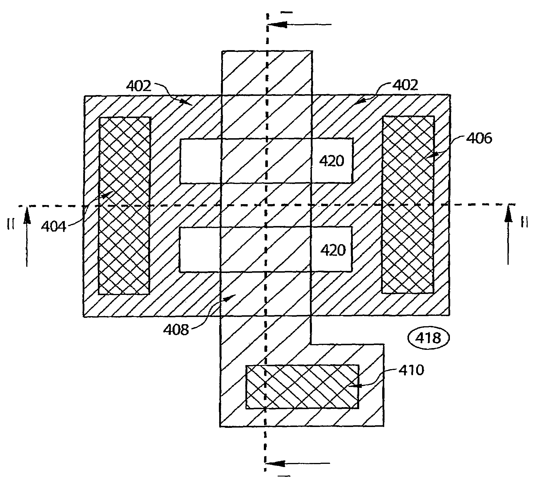
[0028]Referring to FIGS. 4a–c, a field-effect transistor according to a first preferred embodiment of the present invention will be explained subsequently. FIG. 4a shows a top view of the inventive field-effect transistor, wherein FIG. 4b illustrates a sectional view along the section A—A and FIG. 4c illustrates a sectional view along the section B—B.
[0029]The field-effect transistor 400 includes a substrate 402 which can include a homogenous substrate made of a single material or of several layers arranged one above the other. The substrate 402 includes semiconductor materials, such as, for example, silicon or GaAs (gallium arsenide).
[0030]As is illustrated in FIG. 4a, a source terminal electrode 404 and a drain terminal electrode 406 are formed on the semiconductor substrate 402 of the field-effect transistor 400. In the embodiment of the inventive field-effect transistor 400 illustrated in FIG. 4a, the source terminal electrode 404 and the drain terminal electrode 406 are arrange...
PUM
 Abstract
Description
Claims
Application Information