

Method for the removal of an imaging layer from a semiconductor substrate stack
a technology of semiconductor substrates and imaging layers, applied in the field of deep ultraviolet lithography, can solve the problems of increasing the selection of resists to etch conditions for pattern transfer, and increasing the difficulty of etching conditions,
- Summary
- Abstract
- Description
- Claims
- Application Information
AI Technical Summary
Benefits of technology
Problems solved by technology
Method used
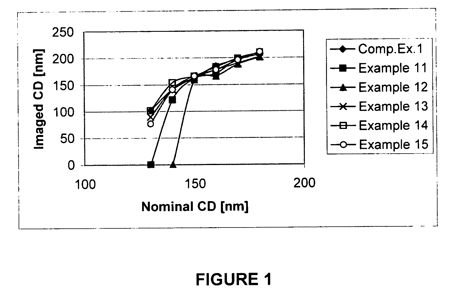
Image

Examples
examples 1 – 8
Examples 1–8
[0103]Examples 1–8 illustrate the rework process with General Procedure 1 for different imaging layer removal solvents. For these examples rework process A with a de-hydration bake of 100° C. for 90 seconds was carried out.
[0104]
TABLE 1Imaging layer removal solvents used and results*ΔCD ofSolvent140 nmRatiotrenchExample #Solvent[weight %](1:1)[%]ProfileComp. 1noneN / A 0%Squaretops, noscumming1PGME / PGMEA / 69.5 / 29.5 / 1.0+0.7%SquareMPKtops, noscumming2PGMEA / EL 90 / 10+2.1%Squaretops, noscumming3PGMEA / MPK 99 / 1+ 18%Footing andscumming4PGMEA100+ 12%Footing andscumming5Cyclohexanone100+1.8%Squaretops, noscumming6Tetrahydrofuran100+4.0%Squaretops, noscumming7n-butyl Acetate100+3.8%Squaretops, noscumming8PGMEA / DMSO 70 / 30+4.0%Squaretops, noscumming*Difference of trench width to comparative example 1
[0105]These results illustrate that lithography after rework is affected differently by different imaging layer removal solvents.
example 9
[0106]This example illustrates the rework process in single wafer mode on track equipment readily available in a semiconductor fabrication plant, without water rinse or de-hydration-bake.
[0107]General Procedure 1 was followed with rework process B and PGMEA as imaging layer removal solvent. This process resulted in after rework images similar to comparative example 1, without scumming or footing. There was, however, some noise in the process and not all wafers were scum free. Trench width of 140 nm trenches after rework were within 3% of the trench width before rework (comparative example 1).
example 10
[0108]This example examines the rework process at a high dehydration bake temperature.
[0109]General Procedure 1 was followed with rework process A and PGMEA as imaging layer removal solvent. A 70 second dehydration bake at 205° C. was employed. The dehydration bake condition was chosen to be identical to the curing conditions for the underlayer.
[0110]Acceptable profiles were observed after re-work and the trench width difference to comparative example 1 was −0.7%. This shows that higher dehydration bake temperatures may be preferred for some solvents (compared to example 4).
PUM
| Property | Measurement | Unit |
|---|---|---|
| temperature | aaaaa | aaaaa |
| temperature | aaaaa | aaaaa |
| temperature | aaaaa | aaaaa |
Abstract
Description
Claims
Application Information