Electron-emitting devices, electron sources, and image-forming apparatus

a technology of electron sources and electron emitting devices, applied in the manufacture of electric discharge tubes/lamps, discharge tubes with screens, discharge tubes luminescnet screens, etc., can solve the problems of increasing driving voltage, large capacitive power consumption, and beam profile expansion, and achieve excellent electron emission efficiency, small capacitance components, and excellent durability

Inactive Publication Date: 2006-03-14
CANON KK
View PDF142 Cites 46 Cited by
  • Summary
  • Abstract
  • Description
  • Claims
  • Application Information

AI Technical Summary

Benefits of technology

[0028]According to the present invention, it is feasible to provide the electron-emitting devices presenting a small electron beam spot on the anode, achieving excellent electron emission efficiency, and having excellent durability, a small capacitance component, and excellent stability. The electron sources using the electron-emitting devices can realize quick responsivity and low power consumption. The image-forming apparatus using the electron sources can provide high-definition images with high luminance over a long period, in addition to the quick responsivity and low power consumption.

Problems solved by technology

Further, the driving voltage was as high as several ten volts, and there was the drawback of large capacitive power consumption because of the configuration.
The Spindt type configuration also had the problem that the beam profile became expanded at the positive electrode (anode).
The foregoing lateral FE configuration had the advantage of capability of reducing the capacitance of the device but had the disadvantage of increasing the driving voltage, because the large distance between the emitter and the gate required several hundred volts for driving.
This configuration also had the problem that the beam profile was expanded at the positive electrode (anode).
It is also conceivable to provide the above Spindt type and lateral FE type electron-emitting devices with a beam focusing means, but this raises problems of complexity in a fabrication method, increase in the device area, decrease in electron emission efficiency, and so on.

Method used


Image

  • Electron-emitting devices, electron sources, and image-forming apparatus
  • Electron-emitting devices, electron sources, and image-forming apparatus
  • Electron-emitting devices, electron sources, and image-forming apparatus

Examples


example 1

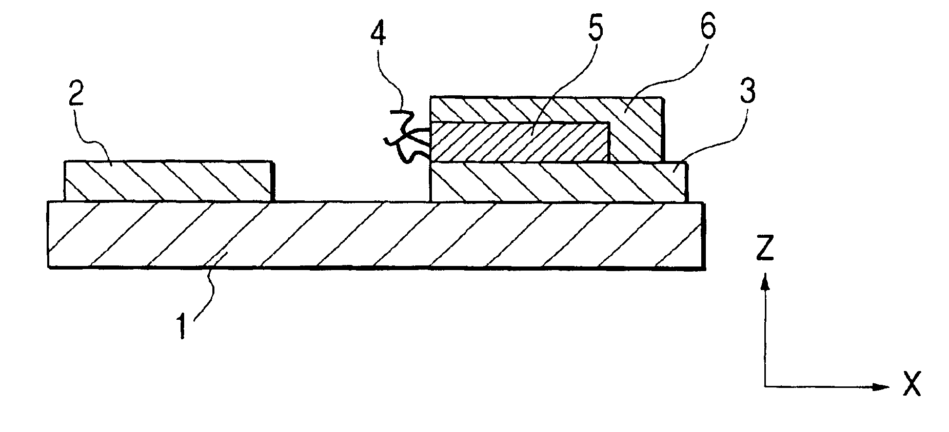
[0174]In the present example, the basic configuration is comprised of the configuration shown in FIGS. 1A and 1B as described in the above-stated embodiment.

[0175]The steps for fabrication of the electron-emitting device according to the present example will be described below in detail with reference to FIGS. 5A to 5E.

(Step 1)

[0176]After a silica substrate used as the substrate 1 was cleaned well, a Ti layer 5 nm thick and a Pt layer 500 nm thick, not shown, were first consecutively evaporated over the entire surface of the substrate by sputtering, in order to form the extraction electrode 2 and the negative electrode 3.

[0177]Then a resist pattern was formed with an unrepresented positive photoresist (AZ1500 available from Clariant) by the photolithography process.

[0178]Using the patterned photoresist as a mask, the Pt layer and Ti layer were then subjected to dry etching with Ar gas to pattern the extraction electrode 2 and the negative electrode 3 with the electrode gap (the widt...

example 2

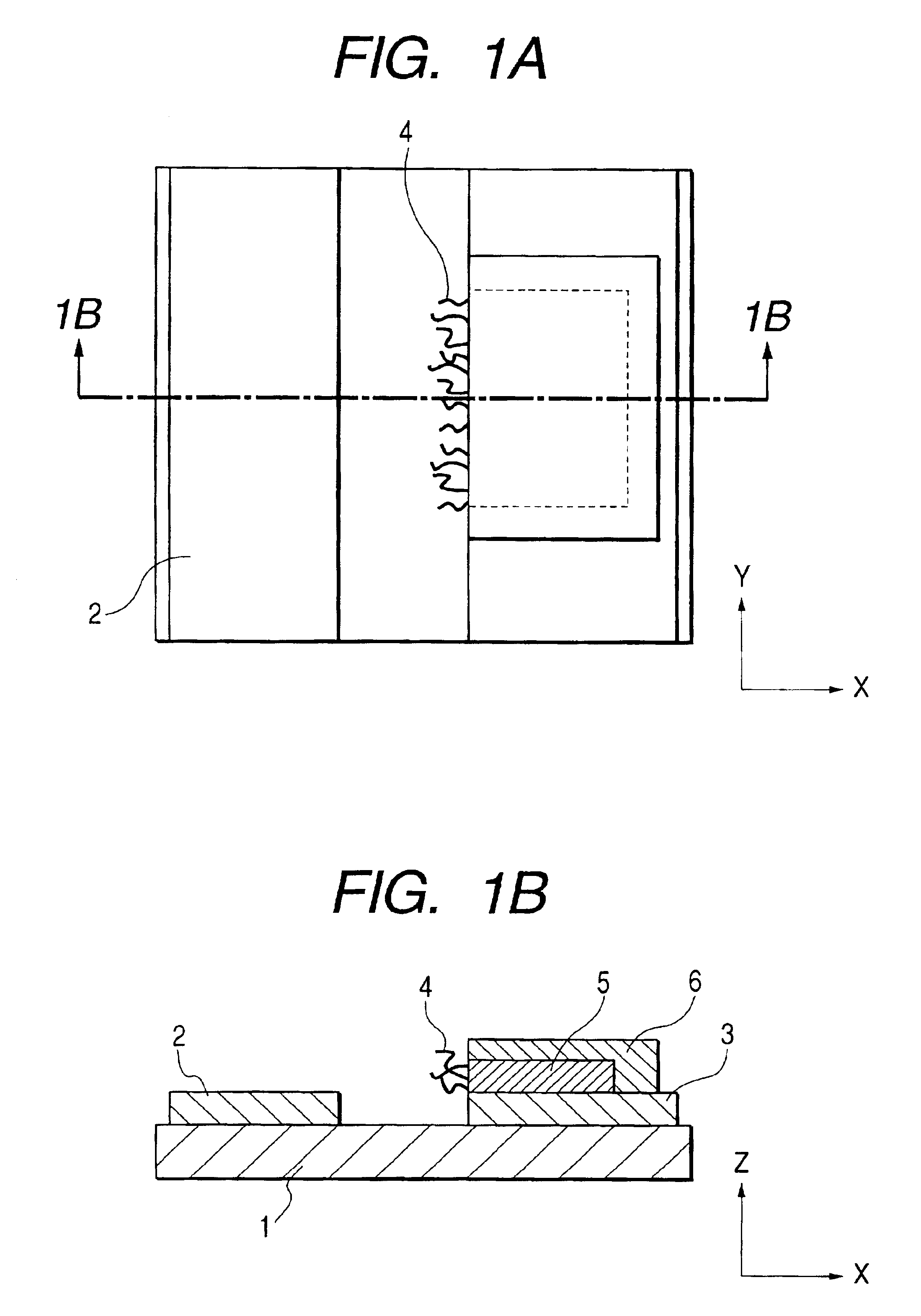
[0201]The electron-emitting device according to Example 2 will be described below with reference to FIGS. 2A and 2B. FIGS. 2A and 2B are schematic views of the electron-emitting device according to Example 2 of the present invention, wherein FIG. 2A is a plan view thereof and FIG. 2B a cross-sectional view along 2B—2B in FIG. 2A.

[0202]The electron-emitting device in the present example was fabricated in the same manner as in Example 1 in the structure and others except that the thickness of the extraction electrode 2 in Example 1 was changed to 200 nm, and If and Ie were measured therewith.

[0203]In the structure of the instant device, the thickness of the negative electrode 3 was larger than the thickness of the extraction electrode 2 whereby the electron emission position was able to be set surely at a higher position (on the anode side) from the extraction electrode 2.

[0204]This configuration decreased the number of electrons flying in the trajectories colliding with the gate, so ...

example 3

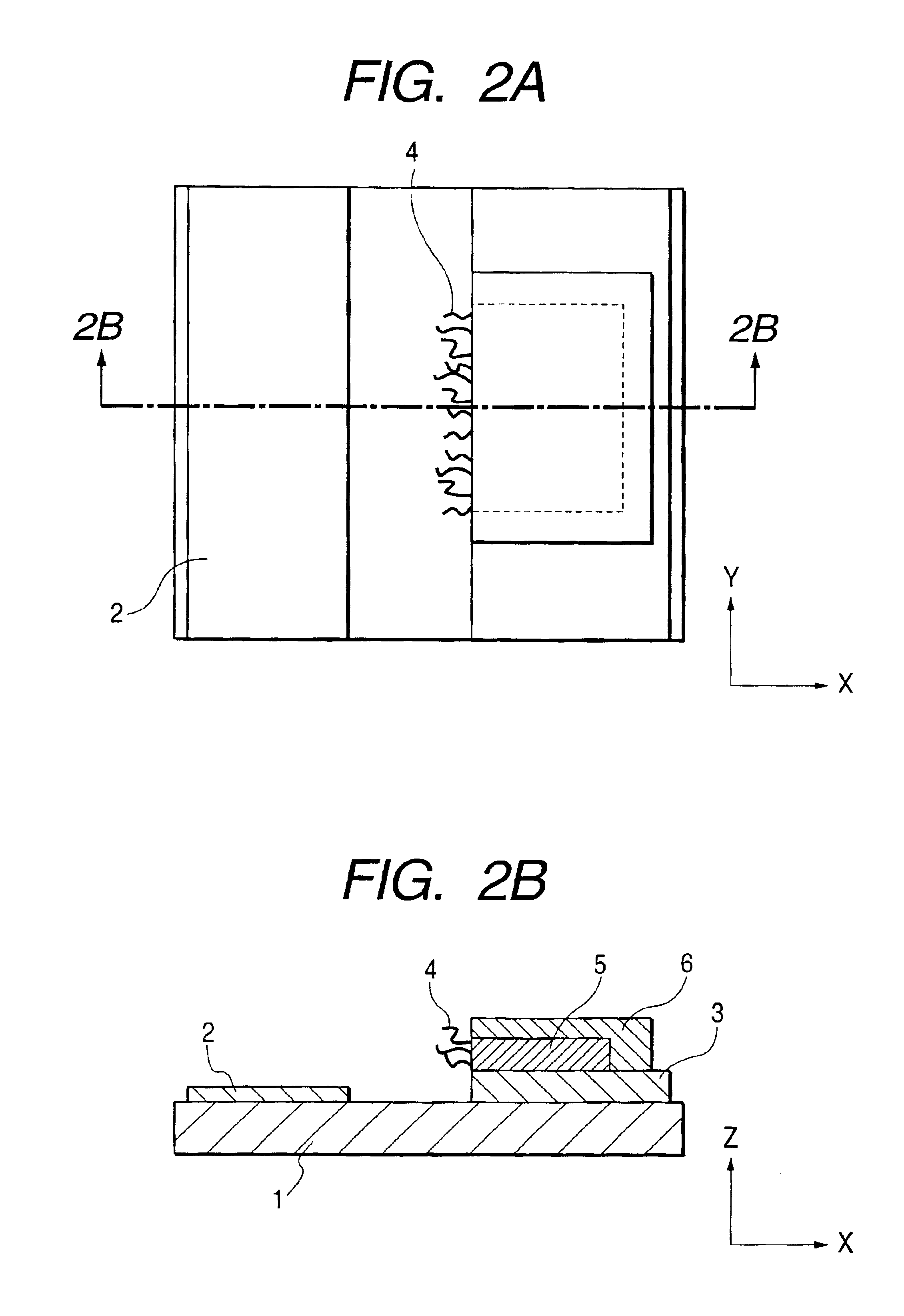
[0207]The electron-emitting device according to Example 3 will be described with reference to FIGS. 3A and 3B. FIGS. 3A and 3B are schematic views of the electron-emitting device according to Example 3 of the present invention, wherein FIG. 3A is a plan view thereof and FIG. 3B a cross-sectional view along 3B—3B in FIG. 3A.

[0208]In the present example, the conductive layer 5 was formed up to an almost middle point of the gap across the gap from on the surface of the negative electrode 3 to on the surface of the substrate in step 2 in Example 1, whereby the gap distance was made to about half.

[0209]Since in the present device the gap distance was smaller than in Example 1, the electric field was about two times stronger than in Example 1. This permitted the voltage for the driving to be reduced to about 8 V. Since the conductive layer 5 was used as an electrical connection layer for the fibrous carbons 4, it became feasible to emit electrons stably from the fibrous carbons 4 in the g...


PUM


Abstract

Provided are electron-emitting devices, electron sources, and image-forming apparatus improved in electron emission efficiency and in convergence of trajectories of emitted electrons. An electron-emitting device has a first electrode and a second electrode placed in opposition to each other with a gap between first and second electrodes on a surface of a substrate, and a plurality of fibers electrically connected to the first electrode and containing carbon as a main component, and the fibers are placed on a surface of the first electrode facing the second electrode.

Description

BACKGROUND OF THE INVENTION[0001]1. Field of the Invention[0002]The present invention relates to electron-emitting devices for emission of electrons, electron sources using them, and image-forming apparatus using the electron sources. The image-forming apparatus according to the present invention can be used in display devices for television broadcasting and the like, display devices of video conference systems, computers, etc., optical printers constructed with use of a photosensitive drum or the like, and so on.[0003]2. Related Background Art[0004]Conventionally, field emission type (FE type) electron-emitting devices configured to apply a strong electric field of not less than 106 V / cm to metal and thereby emit electrons from the metal surface are drawing attention as one of cold electron sources.[0005]If such FE type cold electron sources become practically available, it will become feasible to construct low-profile emissive type image display devices and they will also contribu...

Claims


Application Information

Patent Timeline
Patent Type & Authority Patents(United States)
IPC IPC(8): H01J1/62H01J29/04H01J1/304H01J31/12
CPCB82Y10/00H01J1/304H01J9/025H01J31/127Y10S977/939H01J2201/30469Y10S977/843Y10S977/842
Inventor KAWATE, SHINICHITSUKAMOTO, TAKEO
Owner CANON KK
Why Eureka
Try Eureka